Dust-Free Wipes for Semiconductor Laboratory Cleaning

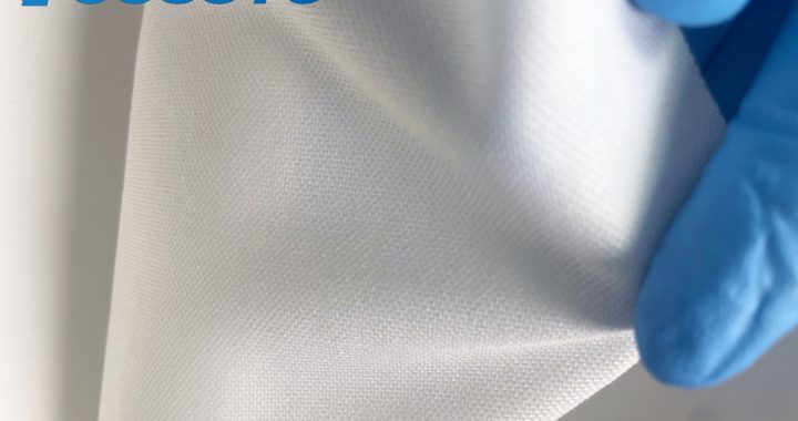
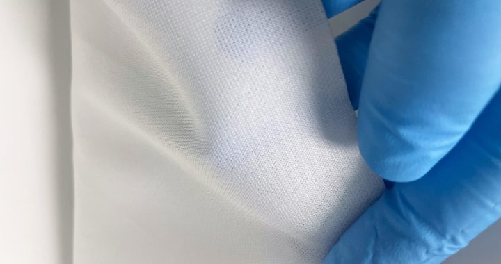
Cleanroom wipes, particularly pre-moistened low-lint types, play a critical role in semiconductor laboratory cleaning processes. They efficiently remove dust, oils, flux residues, and other contaminants from delicate surfaces without generating particles. Proper usage involves selecting the appropriate wipe size, employing gentle unidirectional strokes, and using pre-moistened wipes with isopropyl alcohol or deionized water for heavily soiled areas. Integrating cleanroom wipes into standard cleaning workflows ensures consistent surface cleanliness, protects sensitive semiconductor devices from contamination and ESD damage, and maintains optimal performance and reliability of laboratory equipment.

Features:

  • Lint-free, residue-free, and anti-static for sensitive surfaces

  • Efficient removal of dust, oils, and flux residues

  • Pre-moistened for consistent cleaning performance

  • Safe for semiconductor devices, PCBs, and optical instruments

Application Scope:

  • Semiconductor laboratory surfaces and equipment

  • Cleanroom environments (Class 100–1000)

  • PCB assemblies, wafers, and optical devices

  • ESD-sensitive and precision instrumentation

High-Density Cloth for Semiconductor Cleanroom Cleaning

High-density cleanroom wipes offer significant advantages for maintaining cleanliness in semiconductor cleanrooms. Their tightly woven fibers provide superior particle removal, high liquid absorbency, and lint-free performance, making them ideal for sensitive surfaces and delicate components. These wipes efficiently remove dust, oils, and residues from wafers, PCBs, and precision instruments, reducing contamination risks. Key operational practices include selecting appropriately sized wipes, using gentle unidirectional strokes to prevent particle redistribution, and employing pre-moistened wipes with compatible solvents such as isopropyl alcohol or deionized water. Regular use enhances cleaning efficiency, prolongs equipment lifespan, and ensures consistent high-quality standards in semiconductor manufacturing environments.

Features:

  • High-density fibers for superior particle and contaminant removal

  • Lint-free and residue-free for delicate surfaces

  • High liquid absorption and durability

  • Compatible with IPA, deionized water, and mild solvents

Application Scope:

  • Semiconductor cleanroom surfaces and equipment

  • Wafers, PCBs, and precision instruments

  • Optical devices and sensors in controlled environments

  • ESD-sensitive and delicate manufacturing equipment

High-Density Cloth for Semiconductor Cleaning

High-density cleanroom wipes offer significant advantages for cleaning semiconductor equipment, where maintaining ultra-clean surfaces is critical to process yield and equipment performance. Their tightly woven fiber structure provides superior liquid absorption and particle removal while minimizing lint and residues. These wipes are ideal for cleaning wafers, PCB assemblies, precision instruments, and sensitive semiconductor components. Key operational techniques include using pre-moistened wipes for uniform solvent coverage, applying gentle unidirectional strokes to prevent particle redistribution, and selecting appropriate wipe sizes for different surfaces. Utilizing high-density wipes enhances cleaning efficiency, reduces contamination risks, and ensures reliable performance in semiconductor cleanrooms.

Features:

  • High-density fibers for superior liquid absorption and particle removal

  • Lint-free and residue-free for sensitive surfaces

  • Durable and tear-resistant during rigorous cleaning

  • Compatible with IPA, deionized water, and mild solvents

Application Scope:

  • Semiconductor wafers and PCB assemblies

  • Cleanroom precision instruments and sensors

  • Laboratory and industrial semiconductor equipment

  • Microelectronics and ESD-sensitive components

Pre-Wetted Wipes in Semiconductor Cleanrooms

Pre-moistened cleanroom wipes are essential for maintaining cleanliness in semiconductor cleanrooms, where contamination can critically impact product yield and equipment performance. These wipes are pre-saturated with high-purity solvents, providing consistent coverage to remove dust, oils, fingerprints, and residues without generating lint or particles. Key application techniques include selecting the appropriate wipe size for different surfaces, using gentle unidirectional strokes, and applying multiple wipes for heavily contaminated areas. Pre-moistened wipes are compatible with solvents like isopropyl alcohol and deionized water, ensuring safe use on wafers, PCB assemblies, precision instruments, and other sensitive semiconductor equipment. Proper technique improves cleaning efficiency, reduces contamination risks, and maintains optimal process reliability.

Features:

  • Pre-saturated with high-purity, residue-free solvents

  • Lint-free and low-particulate for sensitive surfaces

  • Consistent coverage for efficient contaminant removal

  • Safe for wafers, PCBs, and semiconductor instruments

Application Scope:

  • Semiconductor cleanroom equipment and work surfaces

  • PCB assemblies and microelectronics

  • Laboratory and precision instruments

  • Wafers and ESD-sensitive components

Anti-Static Cloth for Semiconductor Cleanrooms

Anti-static cleanroom wipes are essential for maintaining cleanliness and preventing electrostatic discharge (ESD) in semiconductor cleanrooms. These wipes are designed to safely remove dust, oils, and residues from sensitive surfaces without generating lint or particles. Their conductive, low-static properties protect semiconductor wafers, PCBs, and precision instruments from ESD damage during cleaning and maintenance. Key operational techniques include using gentle unidirectional strokes, selecting appropriately sized wipes for different surfaces, and employing pre-moistened wipes with compatible solvents such as isopropyl alcohol for stubborn contaminants. Regular use of anti-static wipes ensures high product yield, reduces contamination risks, and maintains the integrity of critical semiconductor processes.

Features:

  • Anti-static and low-lint design

  • Efficiently removes dust, oils, and residues

  • Compatible with IPA and deionized water

  • Protects sensitive semiconductor equipment from ESD

Application Scope:

  • Semiconductor cleanrooms and fabrication areas

  • PCB and wafer handling equipment

  • Precision instruments and sensors

  • ESD-sensitive surfaces and components

High-Density Cloth in Semiconductor Cleaning

High-density cleanroom wipes are designed for precise cleaning of semiconductor equipment, including wafers, photomasks, and assembly tools. Their tightly woven ultra-fine fibers efficiently remove dust, oils, and particulate contaminants without leaving lint or scratches. Compatible with high-purity solvents, these wipes ensure streak-free cleaning, protect sensitive surfaces, and maintain device performance. Ideal for Class 100–1000 cleanrooms, they enhance cleaning efficiency, support contamination control, and optimize semiconductor production workflows.

Features:

  • Ultra-fine, high-density fibers for thorough contaminant removal

  • Lint-free and non-abrasive for sensitive surfaces

  • Excellent solvent absorption for streak-free cleaning

  • Optimized for semiconductor cleanroom applications

Applications/Range:

  • Semiconductor wafers and photomask cleaning

  • Precision tools and equipment maintenance

  • PCB and electronic component cleaning

  • Controlled environment and cleanroom workflows

Case Study: Pre-Wetted Wipes for Semiconductor Cleaning

Pre-wetted cleanroom wipes are widely used for maintaining cleanliness in semiconductor Class 100–1000 cleanrooms. Saturated with high-purity solvents, they effectively remove dust, oils, and particulate contaminants from wafers, photomasks, and precision equipment. Their lint-free, non-abrasive design prevents surface damage and minimizes recontamination. Case studies show that using pre-wetted wipes improves cleaning efficiency, ensures compliance with stringent cleanroom standards, and enhances overall semiconductor production yield and device reliability.

Features:

  • Pre-saturated for uniform and immediate cleaning

  • Lint-free, non-abrasive, and safe for delicate surfaces

  • Efficiently removes dust, oils, and particles

  • Optimized for semiconductor cleanroom workflows

Applications/Range:

  • Semiconductor wafers and photomask cleaning

  • Precision equipment and tools maintenance

  • PCB and electronic component cleaning in cleanrooms

  • Class 100–1000 cleanroom environments

Case Study: High-Density Wipes for Class 100 Cleanrooms

High-density cleanroom wipes are essential for maintaining strict cleanliness standards in Class 100 (ISO 5) environments, providing efficient dust removal without contamination.

Key Features:

  1. High Absorbency: Effectively absorbs dust, liquids, and contaminants, maintaining cleanroom standards.

  2. Lint-Free: Prevents fiber shedding, which is critical in cleanroom environments.

  3. Durability: High-density design offers resistance to tearing, ensuring consistent cleaning performance.

  4. Antistatic Properties: Protects sensitive electronics from static discharge, crucial in Class 100 environments.

Application Range:

  • Semiconductor Manufacturing: Used to clean equipment and workstations without introducing contamination.

  • Pharmaceutical Cleanrooms: Ensures sterility while cleaning surfaces and devices.

  • Optical and Electronics: Used to clean sensitive components like lenses, PCBs, and circuit boards.

  • Biotechnology Labs: Helps maintain a particle-free environment for experiments and equipment.

Best Practices:

  • Unidirectional Wiping: Clean from clean to dirty areas to avoid cross-contamination.

  • Single Use: Dispose of wipes after use to avoid spreading contamination.

  • Regular Monitoring: Inspect cleaned surfaces to ensure no residue or particles are left behind.

  • Proper Storage: Store wipes in sealed packaging to preserve their effectiveness.

Benefits:

  • Maintains Cleanroom Standards: Essential for adhering to Class 100 cleanliness regulations.

  • Prevents Contamination: Lint-free and high-absorbent properties keep sensitive areas clean.

  • Protects Equipment: Antistatic properties safeguard against static discharge, preserving sensitive electronics.

  • Improves Efficiency: Reduces downtime by providing a fast and effective cleaning solution.

Guidelines for Cleanroom Wipes

Cleanroom wipes are crucial in semiconductor manufacturing to maintain particle-free environments and prevent contamination.

Key Features:

  1. Lint-Free: Ensures no fibers are left behind on delicate semiconductor components.

  2. High Absorbency: Effectively captures oils, dust, and other residues without leaving residue.

  3. Antistatic Properties: Minimizes electrostatic discharge (ESD) risks that could damage sensitive electronic components.

  4. Durability: Strong and resilient material ensures wipes remain intact during cleaning processes.

Applications:

  • Wafer Cleaning: Safely removes dust and oils from wafer surfaces without causing contamination.

  • PCB Assembly: Used for cleaning PCBs during assembly, ensuring no residual contamination.

  • Cleanroom Floors and Surfaces: Cleans floors, counters, and equipment surfaces in semiconductor cleanrooms, maintaining particle-free conditions.

  • Microchip Manufacturing: Helps prevent particle contamination on microchips during the manufacturing process.

Best Practices:

  • Unidirectional Wiping: Clean from clean to dirty areas to avoid contaminating previously cleaned surfaces.

  • Use Proper Moisture Levels: Ensure wipes are adequately moistened to avoid excess liquid that could damage equipment.

  • Single-Use Wipes: Discard wipes after each use to prevent cross-contamination.

  • Surface Verification: Check surfaces to ensure they are free of particles and residues after cleaning.

Benefits:

  • Prevents Contamination: Keeps semiconductor devices and equipment free from dust, oils, and static contamination.

  • Protects Sensitive Components: Minimizes the risk of electrostatic discharge (ESD) that can damage microchips and wafers.

  • Improves Cleanroom Standards: Helps maintain the cleanliness required for Class 100 and higher semiconductor cleanrooms.

The role of cleanroom wipes in cleaning semiconductor cleanrooms

Cleanroom wipes are essential in semiconductor cleanrooms for maintaining particle-free environments, protecting sensitive components, and ensuring product quality.

Key Features:

  1. Lint-Free and Non-Abrasive: Prevents scratches and fiber contamination on delicate semiconductor components.

  2. Antistatic Properties: Minimizes electrostatic discharge (ESD) risks during handling and cleaning.

  3. High Absorbency: Efficiently removes dust, oils, and residues from surfaces and tools.

  4. Chemical Compatibility: Safe for use with IPA, deionized water, and approved cleaning solutions.

Applications:

  • Wafer Handling: Cleans surfaces without introducing particles or residues.

  • PCB and Chip Assembly: Maintains cleanliness of sensitive electronics and components.

  • Cleanroom Surfaces: Floors, benches, and instruments in ISO Class 100–1000 environments.

  • Optical and Inspection Equipment: Keeps lenses and microscopes free from contaminants.

Usage Guidelines:

  • Unidirectional Wiping: Use one-way strokes from clean to dirty areas to avoid redistribution.

  • Pre-Wetted vs. Dry Wipes: Pre-wetted for IPA or deionized water for faster cleaning; dry wipes for flexible solvent use.

  • Single-Use Handling: Discard after each task to prevent cross-contamination.

  • Proper Storage: Store in sealed, dust-free containers to maintain cleanliness and moisture.

Benefits:

  • Maintains Semiconductor Cleanroom Standards: Ensures particle-free ISO Class 100–1000 environments.

  • Protects Sensitive Components: Lint-free, non-abrasive, and antistatic wipes reduce damage and ESD risk.

  • Enhances Cleaning Efficiency: High absorbency and optimized material reduce wipe usage and cleaning time.

  • Versatile Application: Suitable for electronics, optics, instruments, and cleanroom surfaces.