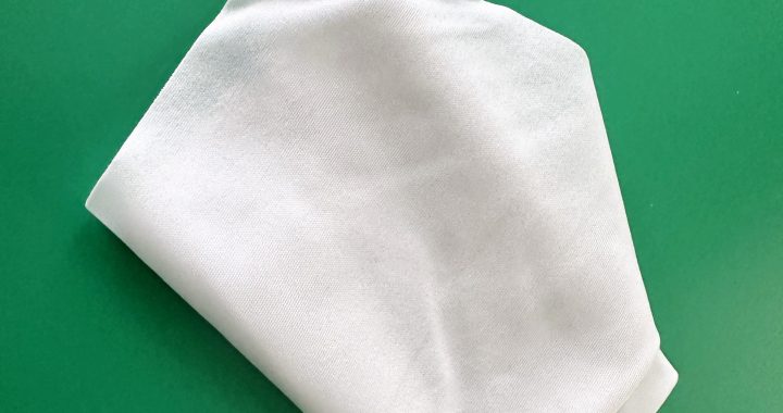
Cleaning wipes are critical in semiconductor cleanrooms to maintain particle-free and ESD-safe environments. Proper techniques ensure effective contamination control and protect sensitive semiconductor components.
Key Features:
-
Lint-Free: Prevents fiber shedding that could damage wafers or devices.
-
High Absorbency: Quickly removes residues, oils, and moisture.
-
Antistatic Properties: Reduces electrostatic discharge (ESD) risks.
-
Durable: Resists tearing for thorough cleaning of critical areas.
Usage Techniques:
-
Unidirectional Wiping: Always wipe in one direction to avoid redepositing particles.
-
Single-Use: Dispose of each wipe after use to prevent cross-contamination.
-
Target High-Risk Areas: Focus on benches, tools, and sensitive equipment first.
-
Pre-Wetted Wipes: Use IPA or deionized water pre-moistened wipes for enhanced cleaning.
Application Range:
-
Semiconductor Wafers: Cleaning surfaces before and after processing.
-
Workstations: Maintaining particle-free benches and tool areas.
-
Optical Components: Lenses and mirrors in semiconductor inspection equipment.
-
Cleanroom Compliance: Supports Class 100–1000 standards for sensitive environments.