Case Study: ESD Wipes in Equipment Maintenance

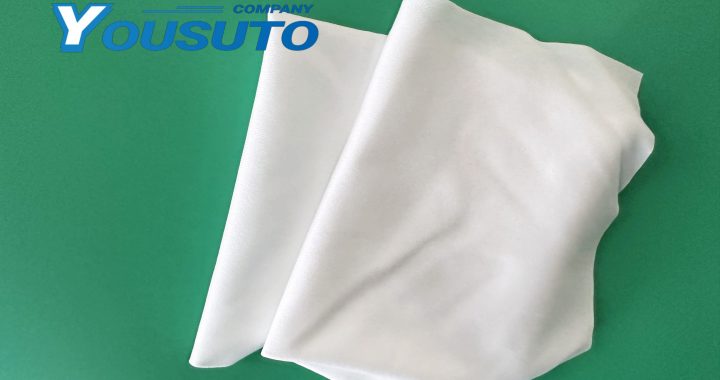
Anti-static cleanroom wipes play a crucial role in maintaining semiconductor equipment. These wipes are designed to be lint-free and possess anti-static properties, preventing electrostatic discharge (ESD) that could potentially damage sensitive semiconductor components. In semiconductor manufacturing and maintenance, these wipes are used to clean wafer surfaces, photomasks, photolithography equipment, and other precision tools. Their pre-saturated form with high-purity solvents ensures thorough cleaning without leaving residues. Proper wiping techniques, such as single-direction strokes and controlled pressure, are essential for removing dust, oils, and residues without harming delicate components. The use of these wipes in Class 100–1000 cleanrooms improves the overall equipment longevity and reliability.

Key Features:

  • Anti-static properties to prevent ESD damage

  • Lint-free for residue-free cleaning

  • Pre-saturated with high-purity solvents for thorough cleaning

  • Safe for delicate semiconductor equipment and components

Application Scope:

  • Semiconductor manufacturing and maintenance

  • Cleanroom environments (Class 100–1000)

  • Wafer surfaces, photomasks, and photolithography equipment

  • Precision tools and high-tech equipment maintenance

Cleaning Wipes for Anti-Static PCB Cleaning

Cleaning wipes are vital tools for preventing electrostatic discharge (ESD) during PCB maintenance in semiconductor laboratories. Pre-wetted or dry lint-free wipes effectively remove dust, oils, flux residues, and microscopic contaminants from delicate PCB surfaces without causing damage. Anti-static properties ensure ESD protection, safeguarding sensitive electronic components. Proper cleaning techniques, including single-direction wiping and controlled pressure, optimize contaminant removal, reduce cleaning time, and minimize solvent usage. These wipes are suitable for Class 100–1000 cleanrooms, ensuring high-quality PCB performance and reliable operation of semiconductor devices.

Key Features:

  • Lint-free and anti-static to prevent ESD and particle attraction

  • Effective removal of dust, oils, and flux residues

  • Compatible with pre-wetted or dry cleaning methods

  • Reduces cleaning time and solvent consumption

Application Scope:

  • Semiconductor laboratory PCB maintenance

  • Cleanroom electronics assembly and inspection

  • Precision PCB and microelectronic device cleaning

  • Industrial and research semiconductor facilities