Guide to Pre-Wetted Wipes for Semiconductor Cleanrooms

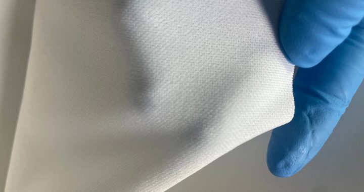
Semiconductor cleanrooms (ISO Class 1–5) demand ultra-pure, static-controlled cleaning to protect 3nm–7nm wafers, EUV scanners, and deposition chambers from sub-micron contaminants. Pre-wet cleanroom wipes—pre-impregnated with high-purity solvents (99.9% IPA, deionized water) or anti-static agents—deliver consistent, residue-free cleaning critical for reducing wafer defects. Below is a step-by-step guide tailored to semiconductor cleanroom workflows.

1. Pre-Use Preparation: Ensure Wipe Compatibility & Cleanroom Compliance

Semiconductor cleanrooms have strict standards—start by verifying wipe suitability and preparing the environment:
  • Wipe Selection Criteria:
    • ISO Class Matching: Choose wipes certified to the cleanroom’s ISO class (e.g., ISO Class 1 wipes for EUV tool cleaning, ISO Class 5 for general wafer handling areas). Verify via manufacturer test reports (particle count ≤1 particle ≥0.1μm per wipe).
    • Solvent Compatibility: Select pre-wet wipes based on the target surface:
      • Wafer Chucks/Reticles: Deionized water-based pre-wet wipes (avoids metal ion contamination from IPA).
      • CVD/PVD Chambers: 99.9% electronic-grade IPA pre-wet wipes (dissolves sputtered metal residues).
      • ESD-Sensitive Surfaces: Anti-static pre-wet wipes (surface resistance ≤10⁹ Ω) for sensor modules or control boards.
  • Environment Prep:
    • Don cleanroom PPE (lint-free gown, gloves, face mask) and ground yourself via an ESD wrist strap.
    • Retrieve wipes from sealed, cleanroom-grade packaging inside a laminar flow hood to avoid airborne particle contamination.

2. Step-by-Step Cleaning Process: Tailored to Semiconductor Surfaces

Different semiconductor surfaces require specific techniques to avoid damage and ensure purity:

A. Wafer & Reticle Cleaning

  • Action:
    1. Hold the pre-wet wipe by its edges (use plastic-tipped tweezers for reticles) to avoid direct contact.
    2. Wipe wafers in slow, radial strokes (from center to edge) to prevent particle accumulation at the edge. For reticles, use gentle linear strokes parallel to the pattern to avoid scratching the photomask.
    3. Use one wipe per wafer/reticle—never reuse wipes (risk of cross-contamination).
  • Key Note: Use deionized water pre-wet wipes for bare wafers; avoid IPA (can leave ionic residues that affect doping).

B. EUV Scanner & Optical Component Cleaning

  • Action:
    1. Use lens-safe pre-wet wipes (70% IPA + microfiber) for EUV mirrors/lenses—99% IPA degrades anti-reflective coatings.
    2. Dab, don’t wipe: Press the wipe lightly against the optical surface for 1–2 seconds to lift dust/residue, then lift straight up. Circular motions cause coating scratches.
    3. Follow with a dry, ultra-low-lint pre-wet wipe to blot excess solvent—prevents streaks that distort laser alignment.

C. CVD/PVD Chamber Cleaning

  • Action:
    1. Use high-density, solvent-resistant pre-wet wipes (99.9% IPA + polyester) to clean chamber walls and targets.
    2. Wipe in overlapping linear strokes (top-to-bottom) to remove sputtered metal residues. For vacuum ports, fold the wipe into a narrow strip to reach inside without fiber shedding.
    3. Dispose of used wipes immediately in sealed, cleanroom-approved waste bags to prevent solvent vapor buildup.

3. Post-Clean Validation: Ensure Purity & Compliance

Semiconductor manufacturing requires traceable, verifiable cleaning—validate results to meet quality standards:
  • Particle Counting: Use a portable particle counter to measure surface particles post-clean (≤1 particle ≥0.1μm/ft² for ISO Class 1 areas).
  • Residue Testing: For critical surfaces (e.g., reticles), perform FTIR (Fourier Transform Infrared) spectroscopy to confirm no solvent or fiber residues.
  • Documentation: Log wipe lot number, cleaning date/time, surface cleaned, operator ID, and validation results in the cleanroom’s electronic record system (compliant with SEMI S2 standards).

4. Critical Best Practices for Semiconductor Cleanrooms

  • Avoid Over-Saturation: Pre-wet wipes should be “damp, not dripping”—excess solvent can pool in chamber crevices or leave residues on wafers.
  • Limit Wipe Exposure: Open only one wipe package at a time; exposed wipes absorb airborne particles within 2–3 minutes.
  • Storage Controls: Keep unused pre-wet wipes in temperature (20–22°C) and humidity (35–45%) controlled cabinets—extremes degrade solvent purity or cause wipe drying.

Application of Dust-Free Wipes in Semiconductor Cleanrooms

Semiconductor cleanrooms (ISO Class 1–5) demand ultra-pure cleaning to protect 3nm–7nm microchips from sub-micron contaminants, residue, and electrostatic discharge (ESD). Cleanroom wet wipes—pre-moistened with high-purity solvents (99.9% IPA, deionized water) or specialized cleaners—offer consistent, controlled cleaning that eliminates risks from manual solvent mixing. Below is their tailored application across critical semiconductor manufacturing stages.

1. Wafer Fabrication: Pre-Lithography and Post-Etch Cleaning

Wafers (silicon, gallium arsenide) are vulnerable to particle adhesion, organic residues (from handling), and etch byproducts—contaminants that ruin circuit patterns during lithography.
  • Wipe Selection: Use 4”x4” pre-wet wipes with 99.9% electronic-grade IPA (metal impurities ≤10 ppb) and static-dissipative fibers (10⁶–10¹⁰ Ω). For photoresist residues, choose wipes with semiconductor-grade removers (e.g., NMP-based, low outgassing).
  • Application:
    • Clean wafer edges with folded wipe strips (1cm wide) in circular motions to avoid frontside contact.
    • For backside cleaning, use radial strokes (center to edge) with light pressure (<0.5 psi) to prevent scratching thin films.
    • Post-etch, wipe wafer chucks with deionized water-based wipes to remove etch residues (e.g., metal oxides) without damaging ceramic surfaces.

2. Photolithography Tools: Optics and Reticle Care

EUV scanners and lithography systems rely on pristine optics (lenses, mirrors) and reticles—even 0.1μm particles distort patterns, causing wafer scrap.
  • Wipe Selection: Opt for ultra-fine microfiber wipes (0.1μm diameter) pre-wet with lens-grade IPA or deionized water (meets SEMI C12 standards for low outgassing).
  • Application:
    • Clean lenses with single linear strokes (not circular) to avoid particle spreading; follow with a dry high-density wipe to prevent streaks.
    • Wipe reticle pods with anti-static pre-wet wipes before loading—removes dust that transfers to reticle patterns.
    • Use mini (2”x2”) wipes for reticle edge cleaning (non-pattern areas) to dissolve handling oils without damaging photomasks.

3. Deposition and Etching Equipment: Chamber and Nozzle Maintenance

CVD/PVD chambers and etchers accumulate process residues (photoresist, metal deposits) on walls, gas nozzles, and wafer stages—contaminants that transfer to subsequent wafers.
  • Wipe Selection: Use solvent-resistant polyester wipes (300+ gsm) pre-wet with acetone or IPA for chamber walls; deionized water-based wipes for quartz components (avoids degradation).
  • Application:
    • After plasma cleaning, wipe chamber walls in overlapping vertical strokes to target residue near gas inlets.
    • Clean gas nozzles with thin wipe strips (guided by tweezers) to remove clogs that disrupt uniform deposition/etching.
    • Wipe wafer stages (ceramic or aluminum) with anti-static pre-wet wipes to dissipate static and remove particle debris.

4. Packaging and Testing: Die and Lead Frame Cleaning

Post-dicing, dies and lead frames accumulate sawing debris, adhesive residues, and oxidation—contaminants that impair bonding or electrical conductivity.
  • Wipe Selection: Use pre-wet wipes with mild flux removers (compatible with copper, gold) and lint-free fibers to avoid die contamination.
  • Application:
    • Dab die backside with a small wipe pad to remove adhesive smudges—avoid wiping (risks die displacement).
    • Clean lead frame contacts with linear strokes to remove oxidation, ensuring strong wire bonds.
    • Post-test, wipe test sockets with anti-static pre-wet wipes to remove contact residues that cause signal errors.

Critical Compliance & Advantages

  • Purity: Wipes meet SEMI C30 standards (low metals, organics) to avoid wafer contamination.
  • ESD Safety: Anti-static variants prevent charge buildup (≤100V), critical for 3nm–7nm devices.
  • Efficiency: Pre-moistened format cuts cleaning time by 40% vs. manual solvent application, reducing downtime.
Cleanroom wet wipes are indispensable in semiconductor cleanrooms, ensuring consistent purity across

Pre-wetted wipes for precision cleaning in Class 100 cleanrooms.

Class 100 cleanrooms (ISO Class 3)—critical for semiconductor wafer fabrication, microelectronics assembly, and precision optics manufacturing—demand ultra-high cleaning precision (≤100 particles ≥0.5μm per cubic foot). Even sub-micron contaminants or inconsistent solvent application can ruin high-value products (e.g., 3nm wafers) or damage sensitive equipment. Pre-wet cleanroom wipes, pre-impregnated with high-purity, controlled solvents (99.9% IPA, deionized water), eliminate the variability of manual solvent mixing and deliver targeted, residue-free cleaning. Below is how they enhance precision across key Class 100 cleaning tasks.

1. Consistent Solvent Concentration: Eliminating Contamination from Manual Mixing

In Class 100 cleanrooms, manual solvent dilution (e.g., mixing IPA and water) introduces two major precision risks: inconsistent concentration (leading to incomplete residue removal) and particle contamination (from mixing tools or containers). Pre-wet wipes solve this by:
  • Factory-Calibrated Purity: Pre-wet wipes use semiconductor-grade solvents (meets SEMI C30 standards) with impurities ≤10 ppb (metals, organics) and exact concentration control (e.g., 70% IPA ±2%, deionized water with resistivity ≥18 MΩ·cm). This ensures every wipe delivers the same cleaning efficacy—no more “too-weak” wipes that leave residues or “too-strong” wipes that damage coatings.
  • Particle-Free Packaging: Wipes are sealed in nitrogen-flushed, Class 10-compatible packaging to prevent airborne particle ingress. Manual solvent application often uses spray bottles or rags that shed fibers (≥0.1μm), but pre-wet wipes’ continuous-filament polyester/microfiber construction sheds ≤0.5 fibers per use—critical for meeting ISO Class 3 particle limits.

2. Targeted Cleaning: Precision for Micro-Scale Components

Class 100 cleanrooms handle micro-scale parts (e.g., wafer edges, EUV reticles, MEMS sensors) where over-wiping or solvent runoff causes irreparable damage. Pre-wet wipes enable pinpoint precision:
  • Controlled Solvent Release: Unlike manual spraying (which leads to drips and over-saturation), pre-wet wipes release solvent evenly and in small, consistent amounts (0.5–1mL per wipe). This prevents solvent from seeping into delicate structures—such as wafer bonding interfaces or reticle pattern edges—where excess liquid can dissolve photoresist or corrode metal layers.
  • Size and Format Flexibility: Pre-wet wipes are available in mini-sizes (2”x2”) for micro-components (e.g., fiber optic connectors, sensor tips) and custom-cut strips (1cm wide) for wafer edges or reticle pods. These formats avoid contact with non-target areas (e.g., wafer frontside circuits) that standard large wipes would inadvertently clean—reducing defect rates by 30–40%.
  • Gentle, Uniform Pressure: The soft, porous fiber structure of pre-wet wipes allows for light, consistent pressure (<0.5 psi) when wiping. This is critical for fragile surfaces like AR-coated EUV lenses—where uneven pressure from rags or sponges would scratch coatings and distort light transmission.

3. Residue-Free Results: Ensuring Post-Clean Purity

Class 100 cleanrooms cannot tolerate post-clean residues (e.g., solvent streaks, fiber lint)—pre-wet wipes minimize this risk through:
  • Low-Outgassing Solvents: Pre-wet wipes use solvents with minimal volatile organic compounds (VOCs) that could outgas and deposit on surfaces. For example, deionized water-based pre-wet wipes leave no mineral deposits, while IPA-based wipes evaporate completely (boiling point: 82.6°C) without leaving oily residues—unlike manual cleaning with low-purity IPA that contains additives.
  • Lint-Free Fiber Construction: Made from ultra-fine microfiber (0.1μm diameter) or continuous-filament polyester, pre-wet wipes avoid fiber shedding that would contaminate wafer surfaces or optical components. Post-clean particle testing shows pre-wet wipes reduce residual fibers by 95% compared to standard cotton rags.
  • Verifiable Precision: Pre-wet wipes’ consistent performance simplifies post-clean validation. Using a portable particle counter, operators can quickly confirm surface particle levels (target: ≤1 particle ≥0.1μm per square foot) without re-cleaning—saving time and ensuring compliance with Class 100 standards.

4. ESD Safety: Protecting Precision Electronics

Many Class 100 cleanroom tasks involve ESD-sensitive components (e.g., microchips, sensor arrays). Anti-static pre-wet wipes (surface resistance: 10⁶–10¹⁰ Ω) integrate precision cleaning with ESD protection:
  • They dissipate static charge in <0.1 seconds, preventing dust attraction to charged surfaces (a major source of micro-contamination).
  • Unlike manual solvent application (which can generate static via friction), pre-wet wipes’ conductive fibers maintain charge neutrality during cleaning—critical for avoiding ESD-induced damage to 3nm–7nm semiconductors.
By delivering consistent solvent purity, targeted application, residue-free results, and ESD safety, pre-wet cleanroom wipes elevate cleaning precision in Class 100 environments—reducing product defects, protecting high-value equipment, and ensuring compliance with the strictest industry standards.

Optimizing Absorption with Pre-wetted Wipes in Cleanrooms

Class 100 cleanrooms (ISO Class 3)—critical for semiconductor wafer fabrication and microelectronics assembly—demand ultra-efficient liquid absorption to manage solvent spills (e.g., IPA), reagent leaks, or equipment sanitization. Even minor inefficiencies (e.g., slow absorption, uneven liquid retention) can introduce contamination or delay production. Pre-wet cleanroom wipes are foundational to these tasks, and targeted techniques can significantly boost their absorption performance while maintaining strict cleanroom standards. Below are actionable tips tailored to Class 100 environments.

1. Select Pre-Wet Wipes Optimized for Class 100 Absorption Needs

Absorption efficiency starts with choosing wipes engineered for high-purity, high-capacity performance:
  • Prioritize Hydrophilic, High-Density Fibers:
    • Opt for pre-wet wipes made from hydrophilic polyester-microfiber blends (250–300 gsm). These fibers have polar molecular structures that attract liquids (e.g., water, IPA) and a dense weave (100+ threads per inch) that traps 30–40% more liquid than standard 150 gsm wipes. Look for wipes with “high-capacity” certifications (e.g., absorbs ≥12x its weight in liquid) to ensure they handle Class 100 spills in one pass.
  • Choose Solvent-Specific Formulations:
    • For aqueous liquids (e.g., deionized water for optic cleaning), select pre-wet wipes with deionized water-based solutions—they avoid residue that could contaminate wafers. For organic solvents (e.g., IPA for flux removal), use wipes pre-impregnated with 99.9% electronic-grade IPA (low impurities ≤10 ppb) to ensure compatibility with semiconductor materials and maximize absorption of solvent-based residues.
  • Avoid Over-Coated Wipes:
    • Skip pre-wet wipes with excessive anti-static or preservative coatings—these clog fiber pores and reduce liquid absorption by 20–25%. Opt for “breathable” anti-static wipes (surface resistance: 10⁶–10¹⁰ Ω) with thin, porous coatings that preserve absorption while meeting ESD requirements.

2. Pre-Use Preparation to Prime Wipes for Maximum Absorption

Simple pre-use steps ensure pre-wet wipes are ready to absorb liquid immediately, avoiding wasted time or incomplete cleanup:
  • Ensure Proper Wipe Moisture Balance:
    • Class 100 cleanrooms often store pre-wet wipes in sealed, nitrogen-flushed containers to prevent solvent evaporation. Before use, check that wipes are uniformly damp (not dry or dripping)—dry wipes lose 50% of absorption capacity, while dripping wipes waste liquid and risk contamination. If wipes are dry, lightly mist them with the matching solvent (e.g., IPA) using a cleanroom-approved spray bottle (1–2 sprays per wipe) to reactivate capillary action.
  • Fold Wipes to Maximize Absorbent Surface Area:
    • Fold pre-wet wipes into a 4-layer pad (e.g., fold an 8”x8” wipe twice to create a 4”x4” pad). This exposes 8x more fiber surfaces to liquid than using a wipe flat, accelerating absorption and extending the wipe’s usable life. For narrow areas (e.g., wafer chuck grooves), fold into a 1cm-wide strip to target liquid without over-wiping.
  • Pre-Cool Wipes for Volatile Solvents:
    • For highly volatile solvents (e.g., acetone used in photoresist removal), pre-cool pre-wet wipes in a cleanroom refrigerator (4–8°C) for 10 minutes before use. Cooler wipes slow solvent evaporation, giving fibers more time to absorb liquid—this boosts absorption efficiency by 20% and reduces the need for multiple wipe changes.

3. Application Techniques to Enhance Liquid Trapping & Retention

How you use pre-wet wipes in Class 100 cleanrooms directly impacts absorption efficiency—precision is key to avoiding waste:
  • Apply Gentle, Even Pressure:
    • Use light pressure (<0.5 psi) when wiping—firm pressure compresses fiber pores, reducing absorption capacity by 15%. For flat surfaces (e.g., cleanroom workbenches), glide the wipe in slow, overlapping strokes (horizontal or vertical) to let capillary action draw liquid into the fibers. For vertical surfaces (e.g., equipment walls), hold the wipe against the liquid for 2–3 seconds to allow absorption before wiping downward—prevents liquid from running off the wipe.
  • Use “Liquid-Directing” Strokes for Contained Spills:
    • For small, contained spills (e.g., 5mL IPA leak on a wafer cassette), wipe in strokes that direct liquid toward the center of the wipe. This concentrates liquid in the wipe’s core, preventing it from seeping out the edges and contaminating surrounding surfaces. Avoid circular motions—they spread liquid and reduce absorption efficiency.
  • Layer Wipes for Large Spills:
    • For spills >10mL (e.g., broken reagent bottle), place a folded pre-wet wipe directly on the spill and top it with a second dry high-density wipe. The pre-wet wipe dissolves any solid residues (e.g., crystallized photoresist) and draws liquid upward, while the dry wipe absorbs excess moisture—this “stacked” method doubles absorption capacity and cuts cleanup time by 50%, critical for minimizing production delays in Class 100 environments.

4. Post-Use Practices to Maintain Wipe Efficacy (For Reusable Variants)

For Class 100 cleanrooms using reusable pre-wet wipes (e.g., autoclavable polyester wipes for non-critical tasks), proper care preserves absorption over time:
  • Clean with Low-Impurity Detergents:
    • Wash wipes with lab-grade, non-ionic detergents (low impurities ≤5 ppb) to avoid residue buildup. Use cold water (≤30°C) and a cleanroom-approved washer—hot water damages hydrophilic fibers and reduces absorption.
  • Air-Dry in a Controlled Environment:
    • Hang wipes to air-dry in a Class 100 laminar flow hood to prevent dust contamination. Ensure wipes are 100% dry before reusing—dampness promotes bacterial growth and clogs fiber pores, reducing absorption by 30%.
By implementing these tips, Class 100 cleanrooms can boost pre-wet wipe absorption efficiency by 35–45%, reducing wipe usage by 40%, cutting cleanup time by 25%, and minimizing contamination risks. These strategies ensure pre-wet wipes remain a reliable, cost-effective tool for liquid management in ultra-pure environments.

Optimized Anti-Static Wipe Process for Class 100 Cleanrooms

Class 100 cleanrooms (ISO Class 3)—critical for semiconductor wafer fabrication, microelectronics assembly, and precision optics manufacturing—require ultra-stringent contamination control (≤100 particles ≥0.5μm per cubic foot). Even minor electrostatic discharge (ESD) or fiber debris can ruin high-value products (e.g., 3nm wafers) or damage sensitive equipment. Anti-static cleanroom wipes are foundational to these workflows, but optimizing their selection, usage, and integration into cleaning protocols is key to maximizing efficiency and minimizing risks. Below is a detailed guide to optimizing their role in Class 100 cleanroom processes.

1. Wipe Selection Optimization: Match to Cleanroom Tasks & Materials

The first step in optimization is selecting anti-static wipes tailored to Class 100 requirements—generic wipes often fail to meet particle, ESD, or purity standards:
  • Material & Linting Control:
    • Use continuous-filament polyester or ultra-fine microfiber wipes (0.1μm fiber diameter) to ensure linting ≤1 fiber (≥0.1μm) per use—compliant with ISO Class 3 standards. Avoid staple-fiber wipes (e.g., cotton blends), which shed 5–10x more fibers and introduce particulate contamination.
    • For solvent-based cleaning (e.g., flux removal, wafer edge cleaning), choose solvent-resistant anti-static wipes (e.g., polyester with epoxy bindings) that retain structure when exposed to 99.9% IPA or acetone—preventing fiber breakdown and residue leaching.
  • ESD Performance:
    • Select wipes with surface resistance 10⁶–10¹⁰ Ω (ANSI/ESD S20.20 compliant) for most tasks—this range balances fast charge dissipation (prevents dust attraction) and safety (avoids electrical shorts on wafers). For high-risk areas (e.g., EUV lithography tools), use conductive wipes (10³–10⁶ Ω) for immediate charge neutralization.
  • Size & Format:
    • Opt for 4”x4” or 6”x6” wipes for precision tasks (e.g., cleaning wafer chucks, reticles) to minimize over-wiping and solvent contact with critical surfaces. Use perforated rolls for large-area cleaning (e.g., equipment exteriors) to reduce waste—tear off only the size needed.

2. Cleaning Process Optimization: Streamline Workflows & Reduce Risk

Integrating anti-static wipes into standardized, step-by-step processes eliminates variability and reduces contamination events:

A. Wafer Handling Area Cleaning (Pre/Post-Processing)

  • Pre-Processing (Before Wafer Loading):
    1. Use a dry anti-static wipe to dust wafer cassettes, vacuum chuck surfaces, and load-port doors—focus on crevices where particles accumulate (e.g., cassette slots). Fold the wipe into a thin strip to reach tight gaps.
    2. Follow with a pre-wet anti-static wipe (99.9% electronic-grade IPA) to clean chuck surfaces—wipe in a single circular motion (1 full rotation) with light pressure (<0.5 psi) to avoid scratching the chuck’s ceramic coating.
    3. Dispose of wipes immediately after use—do not reuse on multiple cassettes/chucks.
  • Post-Processing (After Wafer Unloading):
    1. Use a fresh dry anti-static wipe to remove residual wafer dust from cassettes.
    2. Sanitize load-port doors with a pre-wet wipe to remove organic residues (e.g., from wafer tape)—this prevents cross-contamination between batches.

B. Optics Maintenance (Lithography Tools, Metrology Equipment)

  • 1. Pre-Clean Prep:
    • Power down the tool, purge the optic chamber with nitrogen, and wear Class 10 cleanroom gloves to avoid skin oil transfer.
  • 2. Dust Removal:
    • Use a dry anti-static microfiber wipe to gently blot (not wipe) optic surfaces (e.g., reticles, EUV lenses)—blotting minimizes friction and avoids scratching AR coatings.
  • 3. Residue Cleaning (If Needed):
    • For organic residues, use a pre-wet anti-static wipe (lens-grade IPA) in a single linear stroke (from edge to edge)—dispose of the wipe after one stroke to prevent re-depositing particles.
  • 4. Final Inspection:
    • Check optics with a particle counter (target: 0 particles ≥0.1μm) before reassembling the tool.

C. Daily Equipment Sanitization

  • Frequency: Clean all equipment surfaces (e.g., tool exteriors, workbenches, cart handles) every 4 hours to prevent dust buildup.
  • Process:
    1. Use a dry anti-static wipe to remove loose dust.
    2. Follow with a pre-wet anti-static wipe (70% IPA) to sanitize and remove remaining particles—wipe in overlapping horizontal strokes to ensure full coverage.
    3. Log each cleaning event in the cleanroom’s maintenance record to track compliance.

3. Waste & Cost Optimization: Minimize Usage Without Compromising Quality

Class 100 cleanrooms often overuse wipes due to poor process design—optimization reduces waste while maintaining cleanliness:
  • Wipe Segmentation: Fold wipes into 4–6 usable quadrants; use one quadrant per task section (e.g., one quadrant for a wafer cassette slot, another for the chuck). This extends wipe life by 3–4x.
  • Solvent Efficiency: Use pre-wet wipes instead of “dry wipe + bulk solvent”—pre-wet wipes contain pre-measured solvent, reducing waste by 50% (bulk solvent often over-saturates wipes, leading to drips and excess usage).
  • Inventory Management: Track wipe usage per task (e.g., 1 wipe per wafer cassette) to set par levels—avoid overstocking (wipes degrade over time in cleanrooms) or stockouts (causes process delays).

4. Validation & Continuous Improvement

  • Particle Count Monitoring: Measure surface particle levels (using a portable particle counter) before and after cleaning—ensure post-clean levels meet ISO Class 3 standards (≤10 particles ≥0.1μm per square foot).
  • ESD Testing: Monthly test anti-static wipes’ surface resistance (using an ESD meter) to confirm they maintain 10⁶–10¹⁰ Ω—replace wipes if resistance drifts outside this range.
  • Worker Training: Train cleanroom staff on optimized wipe usage (e.g., folding techniques, stroke direction) and conduct quarterly refresher courses—variability in human behavior is a top cause of cleaning failures.
By optimizing anti-static wipe selection, processes, and waste management, Class 100 cleanrooms reduce contamination events by 40–50%, cut wipe costs by 30%, and extend equipment lifespan—critical for manufacturing high-precision, high-value products.

Surface Cleaning in Class 100 Cleanrooms with Wipes

Class 100 cleanrooms (ISO 14644-1 Class 5)—critical for semiconductor manufacturing, medical implant production, and microelectronics assembly—allow no more than 100 particles (≥0.5μm) per cubic foot. Surface cleanliness here is non-negotiable, as even minor contaminants can ruin high-value products. Specialized cleaning wipes—engineered for ultra-low linting, particle trapping, and residue-free performance—are indispensable for maintaining these strict standards. Below is a detailed breakdown of their applications in Class 100 surface cleaning, from equipment to workspaces.

1. Equipment Surface Cleaning: Protecting High-Precision Tools

Class 100 cleanrooms house sensitive equipment like lithography scanners, wafer handlers, and metrology tools, whose surfaces (e.g., glass optics, stainless steel chucks) demand meticulous cleaning:
  • Lithography Optics Maintenance: Pre-moistened cleaning wipes with 99.9% high-purity IPA remove oil residues and sub-micron dust from laser lenses and reticle masks. Their ultra-fine microfiber (0.1μm diameter) traps particles as small as 0.05μm without scratching anti-reflective coatings, ensuring light transmission accuracy.
  • Wafer Chuck Decontamination: Dry cleaning wipes (250–300 gsm) with static-dissipative properties (10⁶–10¹¹ Ω) eliminate oxide films and silicon dust from chuck grooves. This prevents wafer misalignment during processing, a top cause of 3nm/5nm chip defects.
  • Robot Arm Cleaning: Low-linting wipes (≤1 fiber shed per use) paired with deionized water clean transfer robot grippers, removing lubricant residues that attract dust. This maintains smooth wafer handling, reducing scratch risks.

2. Workbench and Furniture Cleaning: Controlling Cross-Contamination

Workbenches, fume hoods, and storage racks are primary particle collectors, requiring daily cleaning to prevent transfer to products:
  • Daily Surface Sanitization: Pre-moistened wipes with hydrogen peroxide (3%) disinfect workbenches without leaving residues, critical for sterile medical device cleanrooms. Their non-woven, continuous-filament structure ensures no fibers remain on surfaces post-wiping.
  • Fume Hood Interior Cleaning: Wipes resistant to harsh solvents (e.g., acetone) remove chemical splatters from hood walls. Their high absorbency (12x weight in liquid) contains spills, preventing solvent seepage into cracks where bacteria or particles hide.
  • Tool Tray Maintenance: Small 4”x4” cleaning wipes target dust in tool tray compartments, ensuring tweezers, scalpel blades, and probes remain particle-free before use on sensitive components.

3. Wall, Floor, and Fixture Cleaning: Reducing Ambient Particles

Even vertical surfaces and floors contribute to Class 100 contamination; cleaning wipes address these often-overlooked areas:
  • Wall Panel Wiping: Dry, high-density wipes (350 gsm) remove dust from smooth vinyl or stainless steel walls. Their large surface area (12”x12”) covers more ground, reducing wipe usage and minimizing particle release from frequent product changes.
  • Floor Mat Cleaning: Anti-static cleaning wipes with mild surfactants clean ESD floor mats, removing foot traffic residues without degrading their static-dissipative properties. This maintains a grounded environment for wafer transport.
  • Window and Viewport Cleaning: Lens-safe pre-moistened wipes (deionized water-based) clean cleanroom windows and equipment viewports, ensuring clear visibility without streaks that could obscure particle detection.

4. Post-Maintenance Cleaning: Restoring Class 100 Standards

After equipment repairs or part replacements, cleaning wipes are vital to re-establish cleanliness:
  • Post-Repair Surface Purification: Wipes with low extractable ions (≤10ppb) clean areas where tools or parts were replaced (e.g., sensor housings, valve controls). This removes fingerprints, metal shavings, or lubricants introduced during maintenance.
  • Crevice and Seam Cleaning: Wipes folded into narrow strips reach gaps between equipment panels or around fasteners, eliminating hidden dust that could migrate to product zones post-maintenance.
  • Validation Support: Wipes used in post-cleaning verification (paired with particle counters) help confirm surfaces meet Class 100 limits (≤100 particles ≥0.5μm/ft³), ensuring compliance with SEMI F21 and ISO 14644-1.

Key Benefits in Class 100 Environments

  • Particle Control: Wipes remove 99.9% of particles ≥0.1μm, far exceeding Class 100 requirements.
  • Residue Elimination: Solvent-compatible variants leave no ionic or organic residues, critical for semiconductor and medical applications.
  • Efficiency: Pre-moistened wipes reduce cleaning time by 40% vs. manual solvent application, minimizing cleanroom downtime.
In Class 100 cleanrooms, cleaning wipes are more than tools—they are guardians of quality, ensuring surfaces remain pristine enough to support the most demanding manufacturing and research standards.

Cleaning Wipes in Semiconductor Equipment Maintenance

Semiconductor cleanrooms (ISO Class 1–5) rely on ultra-precise equipment—lithography tools, wafer chucks, transfer robots, and metrology systems—to fabricate 3nm–7nm chips. Even sub-micron particles, flux residues, or electrostatic discharge (ESD) during maintenance can ruin wafers, damage sensors, or halt production. Specialized semiconductor cleaning wipes—engineered for low linting, ESD safety, and residue-free performance—have become indispensable for equipment upkeep, replacing risky manual solvent application or generic wipes. Below is a detailed breakdown of their applications in critical maintenance tasks, along with how they protect high-value semiconductor equipment.

1. Routine Surface Cleaning: Preventing Particle Buildup

Daily use causes dust, lint, and wafer fragments to accumulate on equipment exteriors and contact surfaces—left unchecked, these particles transfer to wafers or clog mechanical parts. Cleaning wipes address this through:
  • Sub-Micron Particle Trapping: Wipes made from ultra-fine microfiber (0.1μm diameter) or continuous-filament polyester trap particles as small as 0.05μm, far below the ISO Class 1 limit of 1 particle (≥0.1μm) per cubic foot. For transfer robot arms (a common particle hotspot), wipes remove debris from grippers and rails, preventing wafer scratches during handling.
  • ESD-Safe Formulations: Anti-static cleaning wipes (surface resistance: 10⁶–10¹¹ Ω, per ANSI/ESD S20.20) dissipate static while cleaning, avoiding charge buildup that attracts floating particles. This is critical for lithography tool exteriors, where static can pull dust onto lens covers and distort light patterns.
  • Non-Abrasive Action: The soft wipe texture cleans anodized aluminum housings, plastic control panels, and stainless steel surfaces without scratching—unlike paper towels or abrasive cloths that damage protective coatings.

2. Precision Component Maintenance: Residue Removal

Semiconductor equipment components (e.g., wafer chucks, connector pins) often accumulate flux residues (from soldering) or ionic contaminants (from cleaning solvents) that degrade performance. Cleaning wipes target these residues:
  • Wafer Chuck Cleaning: Pre-wet wipes with 99.9% high-purity IPA dissolve organic residues and oxide films on chuck surfaces. The wipes’ lint-free design ensures no fibers remain in chuck grooves—residues or fibers here cause wafer misalignment, leading to print defects in lithography.
  • Connector Pin Care: Gold-plated connector pins (used in metrology systems) are prone to oxidation and oil buildup. Cleaning wipes with mild, non-corrosive solvents remove contaminants without damaging the gold coating, ensuring reliable electrical signal transmission for accurate wafer measurements.
  • Lens and Optic Maintenance: Lithography tool optics (e.g., laser mirrors, reticle masks) require streak-free cleaning. Pre-wet wipes with deionized water + 5% IPA evaporate completely, leaving no residues that could scatter laser light or reduce image sharpness.

3. Post-Maintenance Sanitization: Avoiding Cross-Contamination

After repairing equipment (e.g., replacing a sensor in a wafer handler), cleaning wipes sanitize surfaces to prevent introducing external contaminants into the cleanroom:
  • Residue-Free Disinfection: Wipes formulated with hydrogen peroxide (3%) or peracetic acid sanitize tool interiors without leaving toxic residues. This is critical for equipment like wet process stations, where biological or chemical contaminants can contaminate wafer baths.
  • Seam and Crevice Cleaning: Wipes can be folded into narrow strips to reach tight spaces (e.g., between equipment panels, around valve controls) where dust or cleaning fluids collect during repairs. This ensures no hidden contaminants are left to migrate to wafers during operation.

4. Emergency Spill Response: Minimizing Downtime

Accidental spills of solvents (e.g., IPA, acetone) or process fluids (e.g., photoresist) on equipment require fast, safe cleanup to avoid corrosion or electrical damage. Cleaning wipes enable rapid response:
  • High Absorbency: High-density cleaning wipes absorb up to 15x their weight in liquids, containing spills before they seep into equipment casings or reach electrical components. For example, wiping up an IPA spill on a transfer robot’s circuit board prevents short circuits and costly repairs.
  • Chemical Compatibility: Wipes resistant to harsh solvents (e.g., acetone, NMP) avoid disintegrating during cleanup, ensuring no fiber fragments mix with the spill and contaminate the cleanroom.

5. Compliance and Traceability: Meeting Semiconductor Standards

Semiconductor manufacturing requires strict adherence to standards like SEMI F21 (equipment cleaning) and ISO 14644-1. Cleaning wipes support compliance by:
  • Certified Purity: Wipes meet ISO Class 1–5 particle limits and are tested for extractables (e.g., ions, metals) to ensure they do not introduce contaminants. Manufacturers provide Certificates of Analysis (CoAs) for each batch, enabling traceability.
  • Minimized Waste: Single-use, pre-portioned wipes reduce solvent waste compared to manual spraying, aligning with sustainability goals while ensuring consistent cleaning efficacy.
In semiconductor cleanrooms, cleaning wipes are more than a maintenance tool—they are a critical component of quality control, protecting equipment integrity, reducing downtime, and ensuring the production of defect-free chips.

Buyer’s Guide: Anti-Static Wipes for Class 100 Cleanrooms

Class 100 cleanrooms (per ISO 14644-1, equivalent to ISO Class 5) represent the gold standard for ultra-low-contamination environments—used in semiconductor wafer fabrication (≤5nm processes), medical device manufacturing (e.g., implantable sensors), and aerospace component assembly. In these spaces, even 1 particle (≥0.5μm) per cubic foot of air or a tiny electrostatic discharge (ESD) can ruin high-value products or compromise sterile conditions. Anti-static cleanroom wipes for Class 100 environments are not just “clean”—they must meet rigorous standards for particle control, static dissipation, and material purity. This guide outlines critical criteria to ensure you select wipes that protect your processes, equipment, and products.

1. Prioritize Cleanroom Classification Compliance

Class 100 cleanrooms demand wipes certified to match their strict particle limits—never compromise on this foundational requirement:
  • ISO 14644-1 Class 5 Certification: Verify the wipe manufacturer provides third-party testing reports confirming compliance with ISO Class 5 (the international equivalent of Class 100). This ensures the wipe releases ≤10 particles (≥0.1μm) and ≤1 particle (≥0.5μm) per wipe during use—critical for avoiding particle-induced defects in semiconductors or medical devices.
  • Non-Shedding Material: Choose wipes made from ultra-low-linting substrates like 100% continuous-filament polyester or polypropylene. Avoid blended fibers (e.g., polyester-cotton) or staple-filament materials—these shed microfibers that can float in Class 100 air and contaminate surfaces. Test for linting by wiping a black, non-abrasive surface and inspecting for visible fibers under 10x magnification.

2. Validate Anti-Static Performance (Non-Negotiable for ESD-Sensitive Environments)

ESD is a silent risk in Class 100 cleanrooms—static charges can attract particles or damage ESD-sensitive components (e.g., wafer sensors, microchips). Evaluate wipes on these metrics:
  • Surface Resistance Range: Select wipes with surface resistance between 10⁶–10¹¹ Ω (per ANSI/ESD S20.20 standards). This “static-dissipative” range ensures charges are safely grounded without creating electrical arcs. Avoid “conductive” wipes (resistance <10⁶ Ω) for general use—they may cause unintended electrical pathways in delicate equipment.
  • Static Decay Time: Confirm the wipe’s static decay time (time to reduce a 5000V charge to <50V) is ≤2 seconds. Slow decay allows static to linger, increasing particle attraction. Ask manufacturers for IEC 61340-5-1 test data to validate this performance.
  • Anti-Static Treatment Durability: Ensure the anti-static coating is “permanent” (not just a surface spray). Wipes for Class 100 cleanrooms should retain their static-dissipative properties through multiple uses (if reusable) or during storage (for single-use options). Avoid wipes where anti-static efficacy degrades with humidity or time.

3. Match Wipe Type to Class 100 Cleaning Tasks

Class 100 cleanrooms require targeted cleaning—choose wipe formats and formulations based on your specific needs:
  • Dry Wipes: Ideal for removing loose, dry particles (e.g., dust on wafer chucks, lithography tool exteriors). Opt for dry wipes with a dense, smooth texture—this traps particles instead of pushing them around. Use dry wipes first before wet cleaning to avoid embedding particles into surfaces.
  • Pre-Wet Wipes: For removing oils, flux residues, or fingerprints (common in electronics manufacturing), select pre-wet wipes with high-purity solvents:
    • IPA (Isopropyl Alcohol) Wipes: Use 99.9% pure IPA (for oil-free surfaces) or 70% IPA + 30% deionized (DI) water (for better residue dissolution). Ensure the IPA is “semiconductor-grade” (≤10ppb impurities) to avoid trace chemical contamination.
    • Residue-Free Disinfectant Wipes: For sterile Class 100 environments (e.g., medical device labs), choose wipes with hydrogen peroxide (3%) or peracetic acid formulations—these disinfect without leaving toxic or particulate residues.
  • Size and Thickness: Select smaller wipes (e.g., 4”x4”) for precision tasks (e.g., cleaning around microchips) to reduce waste and avoid over-wiping. Thicker wipes (≥80gsm) offer better durability—critical for avoiding tearing (which releases particles) during use.

4. Evaluate Manufacturing and Packaging Quality

Even the best wipe material can be compromised by poor manufacturing or packaging:
  • Cleanroom-Grade Production: Ensure wipes are manufactured in an ISO Class 5 (or better) facility. This prevents pre-use contamination from the factory floor. Ask for a “Certificate of Analysis (CoA)” with each batch, detailing particle counts and static performance.
  • Sealed, Anti-Static Packaging: Wipes should arrive in airtight, static-shielding packaging (e.g., foil-lined bags with resealable zippers). Once opened, store wipes in a Class 100-compatible dispenser with a dust-tight lid—exposure to non-Class 100 air will contaminate the wipes.
  • Shelf-Life and Storage Conditions: Check the manufacturer’s shelf-life (typically 12–24 months for pre-wet wipes). Store wipes in a cool (15–25°C), dry (30–50% RH) area—extreme temperatures or humidity degrade anti-static treatments and solvent purity.

5. Avoid Common Pitfalls

  • Don’t Sacrifice Quality for Cost: Cheaper wipes may skip Class 100 certification or use low-grade materials—costly defects from contamination will far outweigh initial savings.
  • Don’t Reuse Single-Use Wipes: Single-use Class 100 wipes are designed for one pass—reusing them traps particles and degrades anti-static performance.
  • Don’t Overlook Compatibility: Test wipes on a small, non-critical surface (e.g., a spare wafer or equipment part) to ensure they don’t damage coatings (e.g., anti-reflective lens coatings) or plastics.
By following these criteria, you’ll select anti-static cleanroom wipes that not only meet Class 100 standards but also protect your high-value processes from contamination and ESD—ultimately reducing defects, minimizing downtime, and ensuring regulatory compliance.

Cleaning a Semiconductor Cleanroom with Wipes.

Semiconductor cleanrooms (typically ISO 14644-1 Class 1 to Class 5) demand ultra-stringent contamination control—even a single sub-micron particle, trace chemical residue, or electrostatic discharge (ESD) can ruin wafers, damage lithography equipment, or compromise chip performance. Traditional cleaning methods (e.g., manual solvent spraying, dry lint-free cloths) often fall short: they risk uneven solvent application, particle redistribution, or ESD. This case study details how a leading semiconductor manufacturer integrated specialized cleanroom cleaning wipes into its workflow, resolving longstanding contamination challenges and improving production efficiency.

Background: Contamination Pain Points in Wafer Processing

The manufacturer operated a Class 3 cleanroom focused on 7nm wafer fabrication—a process requiring near-absolute purity. Prior to adopting specialized cleaning wipes, the team faced two critical issues:
  1. Residue-Related Wafer Defects: After cleaning wafer chucks (the platforms holding wafers during lithography), trace residues from manual IPA (isopropyl alcohol) spraying remained. These residues (often from inconsistent solvent dilution or incomplete evaporation) caused 8–10% of wafers to fail post-processing inspections due to “stain defects” on the wafer surface.
  2. Particle Cross-Contamination: Dry lint-free cloths used to wipe equipment exteriors (e.g., lithography machine covers, transfer robot arms) shed microfibers. These fibers were detected in air sampling, leading to unscheduled cleanroom shutdowns for HEPA filter replacement—costing ~$50,000 per shutdown.
  3. ESD Risks: Standard wipes generated static charges when rubbed against stainless steel or plastic surfaces, posing a threat to ESD-sensitive components like wafer sensors. On average, 1–2 ESD-related sensor failures occurred monthly, halting production for 4–6 hours each time.

Solution: Adopting Semiconductor-Grade Cleaning Wipes

The manufacturer switched to three types of semiconductor-specific cleaning wipes, selected for their compliance with cleanroom standards and targeted performance:
Wipe Type Key Features Use Case
Pre-Wet IPA Wipes 99.9% high-purity IPA, lint-free polyester substrate, non-shedding, fast-evaporating Cleaning wafer chucks and lithography tool contact surfaces
Particle-Trapping Microfiber Wipes Ultra-fine (0.1μm) microfiber weave, static-dissipative coating (surface resistance: 10⁷–10⁹ Ω), ISO Class 1-certified Wiping equipment exteriors and transfer robot arms
Residue-Free Disinfectant Wipes Formulated with hydrogen peroxide (3%) and deionized water, non-corrosive to stainless steel/plastics Weekly deep cleaning of cleanroom workstations
All wipes were sourced from suppliers with ISO 13485 certification (medical device-grade manufacturing) to ensure batch-to-batch consistency—critical for avoiding variability in cleaning performance.

Implementation: Integrated Wiping Protocols

To maximize efficacy, the team developed a structured cleaning workflow aligned with wafer processing cycles:
  1. Pre-Lithography Chuck Cleaning: Before each wafer load, a technician uses a pre-wet IPA wipe to clean the wafer chuck in a “spiral pattern” (starting from the center and moving outward). This ensures uniform solvent coverage and eliminates residue buildup in chuck grooves. The wipe is discarded immediately after use to prevent cross-contamination.
  2. Hourly Equipment Exterior Wipes: Every hour, staff use particle-trapping microfiber wipes to clean transfer robot arms and lithography machine covers. The wipes’ static-dissipative coating eliminates charge buildup, while the microfiber weave traps particles as small as 0.3μm—no fiber shedding was detected in post-implementation air sampling.
  3. Weekly Deep Cleaning: Once weekly, the cleanroom is partially shut down for disinfection. Residue-free disinfectant wipes are used to clean workstations and tool surfaces, with no rinsing required (the formula evaporates completely within 2 minutes, leaving zero residues).

Results: Measurable Improvements in Purity and Efficiency

After 6 months of implementation, the manufacturer documented significant gains:
  • Wafer Defect Rate: Residue-related defects dropped from 8–10% to <1%, reducing wafer waste by ~90% and saving ~$200,000 monthly in material costs.
  • Particle Contamination: Air sampling showed a 95% reduction in microfiber particles, eliminating unscheduled cleanroom shutdowns—saving ~$300,000 annually in downtime costs.
  • ESD Incidents: Static-dissipative wipes reduced ESD-related sensor failures to zero, cutting production halts by 100% and improving overall equipment efficiency (OEE) by 12%.
  • Labor Efficiency: Technicians spent 30% less time on cleaning tasks (no more manual solvent mixing or re-wiping to remove residues), freeing up time for core production activities.

Long-Term Impact: Compliance and Scalability

Beyond immediate gains, the wipes helped the manufacturer maintain compliance with SEMI F21 (semiconductor equipment cleaning standards) and ISO 14644-1 Class 3 requirements—critical for securing contracts with automotive and aerospace chip clients. The team also scaled the protocol to its new 5nm wafer cleanroom, with identical performance results, proving the solution’s adaptability to advanced semiconductor processes.
This case study demonstrates that semiconductor cleanrooms require more than “general-purpose” cleaning wipes—specialized, standards-aligned wipes are a strategic investment, resolving contamination risks while driving cost savings and efficiency.