Case Studies: Cleaning Wipes in Semiconductor Cleanrooms

Cleaning wipes are critical in semiconductor cleanrooms to maintain particle-free surfaces, protect sensitive devices, and comply with strict ISO standards.

Key Features:

  1. Lint-Free and Non-Abrasive: Prevents fiber contamination and scratches on delicate wafers and PCBs.

  2. Antistatic Properties: Reduces electrostatic discharge (ESD) risks for sensitive semiconductor components.

  3. High Absorbency: Efficiently removes oils, dust, and residues with fewer wipes.

  4. Chemical Compatibility: Safe for use with IPA, deionized water, and approved cleaning agents.

Application Case:

  • Wafer Cleaning: Wipes remove microscopic particles and residues without damaging surfaces.

  • PCB Maintenance: Efficiently cleans flux residues and dust during assembly and inspection.

  • Semiconductor Equipment: Maintains particle-free workstations and handling tools.

  • Optical Inspection: Keeps sensors and lenses clean for accurate measurements.

Benefits:

  • Maintains Cleanroom Standards: Supports ISO Class 100–1000 compliance.

  • Protects Sensitive Devices: Antistatic, lint-free wipes reduce ESD and contamination.

  • Improves Efficiency: High absorbency and pre-wetted options streamline cleaning tasks.

  • Reduces Cross-Contamination: Single-use wipes ensure safe, residue-free cleaning.

High-Density Wipes for Semiconductor Manufacturing

High-density cleanroom wipes are critical in semiconductor manufacturing, where particle control and surface cleanliness directly affect yield and device performance.

Key Features:

  1. Tightly Woven Fibers: Capture microscopic particles to maintain ultra-clean surfaces.

  2. High Absorbency: Efficiently removes residues, oils, and spills from sensitive wafers and equipment.

  3. Lint-Free and Non-Abrasive: Protects delicate wafers, photomasks, and semiconductor components.

  4. Chemical Compatibility: Resistant to IPA, deionized water, and other approved cleaning agents.

Applications:

  • Wafer Cleaning: Removes particles and residues without scratching surfaces.

  • Photomask Maintenance: Ensures precise patterning by eliminating contaminants.

  • Equipment Wiping: Cleans tools, benches, and robotic arms in production lines.

  • Cleanroom Surfaces: Maintains ISO Class 1–5 standards in semiconductor fabs.

Benefits:

  • Enhanced Yield and Quality: Reduces defects caused by particle contamination.

  • Protects Sensitive Components: Non-abrasive and lint-free construction prevents damage.

  • Improves Cleaning Efficiency: High absorbency decreases wipe consumption and labor.

100% Polyester Knit Wiper is an efficient wiper designed for cleanroom environments, featuring sealed edges and a patented surface treatment technology that effectively captures and retains particulate contamination. Made from 100% continuous filament polyester knit, it offers excellent abrasion resistance and liquid absorbency, making it ideal for ISO Class 3 and higher cleanroom environments. The sealed edge design minimizes fiber contamination, ensuring cleanliness and high efficiency during surface cleaning.

The Role of Anti-Static Wipes in Semiconductor Manufacturing

Antistatic cleanroom wipes are essential in semiconductor production, where even tiny particles or electrostatic discharges (ESD) can damage delicate components and reduce yield. These wipes ensure cleanliness, safety, and efficiency throughout the manufacturing process.

Key Features:

  1. Antistatic Protection: Prevents electrostatic discharge, protecting sensitive semiconductors, wafers, and electronic components from ESD-related failures.

  2. Lint-Free and Non-Abrasive: Ensures no fiber shedding or scratches, maintaining the integrity of delicate surfaces.

  3. High Absorbency: Captures dust, oils, and residues effectively, reducing contamination risk on critical components.

  4. Chemical Resistance: Compatible with solvents like IPA, deionized water, and other cleaning agents used in semiconductor manufacturing.

Applications:

  • Wafer Handling: Maintains particle-free surfaces during wafer processing and inspection.

  • PCB Cleaning: Removes dust, oils, and residues from printed circuit boards without causing damage.

  • Semiconductor Assembly: Protects microchips and delicate components during assembly and testing.

  • Cleanroom Maintenance: Ensures Class 100 or higher cleanroom surfaces remain contaminant-free.

Benefits:

  • Reduces ESD Risks: Protects high-value components from static-related failures.

  • Maintains Cleanliness Standards: Lint-free and absorbent wipes prevent particle contamination.

  • Enhances Production Yield: Cleaner surfaces and controlled ESD lead to higher reliability and quality.

Uster Swabs: Precision Cleaning Breakthrough

In industries with stringent cleanliness requirements such as semiconductor manufacturing, medical device maintenance, and optical instrument care, Uster cleanroom swabs have emerged as a benchmark tool for achieving efficient and contamination-free cleaning. Combining cutting-edge technology with multi-industry needs, these swabs offer a reliable and versatile solution for precision cleaning.

Core Technical Advantages: Precision, Efficiency, and Zero Contamination

  1. Premium Materials Tackling Complex Cleaning Challenges
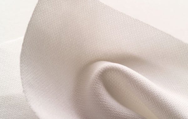
    The swab tips are made from high-performance polyester fibers or polyurethane sponge. The polyester fiber tips offer excellent absorption, while the sponge tips provide strong liquid retention. Different materials suit various applications, allowing the swabs to reach narrow gaps and irregular surfaces. The cushioning effect also prevents mechanical damage to sensitive components like semiconductor wafers and optical lenses. For larger surface areas, wide-head swabs are available.

  2. Thermal Bonding Process Eliminates Secondary Contamination Risks
    Unlike traditional swabs that may leave adhesive residues or shed fibers, Uster swabs use advanced thermal bonding to seamlessly fix the tip materials to polypropylene shafts. This method ensures no adhesive contamination or fiber shedding occurs, and the strong bond withstands repeated wiping and solvent exposure, maintaining cleaning purity.

  3. ISO Class 5 Cleanroom Certification Meets Highest Standards
    Processed through proprietary cleanroom techniques, these swabs exhibit particle emissions and non-volatile residue (NVR) levels far below industry norms, fully complying with ISO Class 5 cleanroom requirements. They effectively maintain a contamination-free environment in chip production and medical instrument sterilization.

  4. Excellent Chemical Resistance for Extreme Cleaning Conditions
    The swab tips resist harsh solvents such as acetone, isopropanol (IPA), and methyl ethyl ketone (MEK), excelling at removing stubborn grease, solder flux residues, and biological contaminants while maintaining structural integrity to prevent tool degradation.

  5. No-Marking Cleaning Technology Protects Delicate Surfaces
    Optimized fiber density and elasticity enable controlled wiping pressure without scratching delicate surfaces like optical coatings and hard disk heads, significantly reducing the risk of scrapped high-precision equipment.

Versatile Applications Across Multiple Fields

  1. Optics and Semiconductor Industries
    Quickly removes lens watermarks, wafer particles, and photoresist residues, while preventing micro-scratches common with traditional swabs, safeguarding optical system imaging quality and chip yield.

  2. Industrial Manufacturing and Electronics Assembly
    Compatible with various industrial solvents, effectively cleans PCB solder points and injection-mold release agents, becoming a standard tool in cleanroom environments.

  3. Medical and Healthcare Sectors
    Meets medical device pre-sterilization cleaning standards, thoroughly removing adhesive residues and biological debris from surgical instruments, supporting GMP compliance for hospitals and IVD equipment manufacturers.

  4. High-End Equipment Maintenance
    An upgraded alternative to conventional cotton swabs, its low fiber shedding prevents secondary contamination during cleaning, widely used for aerospace precision components and laboratory analytical instruments.

Conclusion:
Driven by technological innovation, Uster cleanroom swabs upgrade cleaning standards by addressing traditional tools’ limitations in cleanliness, durability, and applicability. Through rigorous quality control and full lifecycle management, they provide trusted cleaning solutions for critical processes in semiconductors, biomedicine, medical equipment, and beyond, propelling precision manufacturing into a new era of cleanliness.