1. Post-Soldering/Desoldering Cleanup: Removing Flux and Solder Residues
- Application Process:
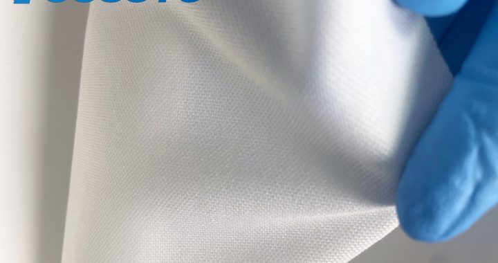
Use pre-wet polyester wet wipes impregnated with 99% electronic-grade IPA. For fresh flux, wipe the soldered area in slow, linear strokes (parallel to copper traces) to dissolve residues; for dried flux, hold the wipe against the spot for 2–3 seconds to soften it before wiping. For fine-pitch components (e.g., QFP chips with 0.5mm pin spacing), tear the wipe into narrow strips to clean between pins without bending leads.
- Key Benefit: Prevents flux-induced corrosion (common in humid lab environments) and ensures reliable electrical contact—critical for test PCBs used in data acquisition systems.
2. Routine Dust and Oil Removal: Preserving PCB Functionality
- Application Process:
For routine maintenance, use pre-wet microfiber wet wipes with 70% IPA. Gently wipe the entire PCB surface, focusing on high-risk areas: edge connectors (dust blocks signal transfer), component leads (oil causes poor solderability), and sensor pads (dust distorts readings). For PCBs mounted in enclosures, use mini pre-wet wipes to reach gaps between the PCB and housing.
- Key Benefit: Extends PCB lifespan by 50–70% vs. infrequent cleaning, reducing the need for costly prototype replacements or test equipment downtime.
3. Sample Spatter and Chemical Contamination Cleaning: Protecting Sensitive Components
- Application Process:
For aqueous splatters (e.g., buffer solutions), use pre-wet cellulose-polyester wet wipes with deionized water to wipe the area immediately—prevents mineral deposits. For organic solvent splatters (e.g., acetone, ethanol), use IPA-impregnated pre-wet wipes to neutralize and remove residues. For biological samples (e.g., cell culture media), use pre-wet wipes with mild, non-toxic disinfectants (compatible with PCBs) to avoid biofilm formation.
- Key Benefit: Protects sensitive components like microcontrollers or sensor chips from chemical damage, ensuring accurate test results from lab equipment.
4. Pre-Storage and Pre-Testing Preparation: Ensuring PCB Readiness
- Application Process:
Pre-storage: Clean the PCB with a dry pre-wet wipe to remove dust, then a light IPA pre-wet wipe to degrease—this prevents corrosion during storage. Place the cleaned PCB in an anti-static bag with a desiccant packet.
Pre-testing: Use a low-lint pre-wet wipe to clean test points and connectors—ensures no contaminants interfere with multimeter or oscilloscope readings, avoiding false positives/negatives in circuit testing.
- Key Benefit: Guarantees PCB reliability when retrieved from storage or tested, minimizing delays in lab experiments or prototype development.