1. Match Pre-Wet Wipes to PCB Contaminant Type
- Flux Residues (Rosin/Cream Solder):
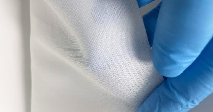
Use pre-wet wipes with 99% electronic-grade IPA (high solvent strength dissolves rosin quickly) or dedicated flux-removing solvents (e.g., semi-aqueous cleaners for “no-clean” flux). Look for wipes with lint-free polyester fibers—they trap dissolved flux without leaving fibers on fine-pitch pads (0.4mm or smaller).
- Solder Spatter/Metal Debris:
Opt for high-density pre-wet wipes (300+ gsm). Their thick, durable fibers capture small solder balls or copper shavings (common post-drilling) without tearing, avoiding the need to switch between wipes for residue and debris.
- Handling Oils/Fingerprints:
Choose pre-wet wipes with 70% IPA (balances solvent power and surface safety). The lower concentration evaporates slower, giving time to dissolve oils on PCB surfaces (e.g., edge connectors, component leads) without damaging solder masks.
- Tip: Label wipe containers by contaminant type (e.g., “Flux Wipes,” “Oil Wipes”) near cleaning stations—this cuts time spent identifying the right wipe.
2. Optimize Wipe Handling for Targeted, Fast Cleaning
- Fold Wipes for Precision & Reusability:
Fold pre-wet wipes into a 4-layer pad (e.g., 8”x8” → 4”x4”) to create multiple “clean surfaces.” Use one layer per PCB section (e.g., one layer for a BGA area, a new layer for edge connectors) —this reduces the number of wipes used per PCB by 30–40% and avoids re-depositing residue.
- Use Strip Cutting for Fine-Pitch Areas:
For PCBs with dense components (e.g., QFP chips, SMD arrays), cut pre-wet wipes into 1cm-wide strips. The narrow shape lets you clean between component leads or under BGA underfill without wiping adjacent parts—saves 15–20 seconds per dense section vs. using full-size wipes.
- Adopt “Linear Stroke” Cleaning for Large Zones:
For open PCB areas (e.g., ground planes, empty pad arrays), wipe in slow, continuous linear strokes (parallel to PCB traces). This avoids back-and-forth motions (which spread residue) and covers more surface area per pass—cuts cleaning time for large PCBs by 25%.
3. Pre-Treat Stubborn Residues to Avoid Scrubbing
- Damp Hold for Dried Flux:
Press a pre-wet flux-removing wipe against dried flux spots (e.g., around old solder joints) and hold for 2–3 seconds. The solvent penetrates the flux, allowing you to wipe it away in one stroke instead of scrubbing repeatedly.
- Blot First for Solder Spatter:
For large solder balls, use a dry corner of the pre-wet wipe to blot excess spatter first—wetting immediately can spread molten solder (if post-rework) or push spatter into component gaps. Blotting takes 5 seconds but avoids 1–2 minutes of picking out trapped debris.
- Use Tweezer-Assisted Wiping for Tight Gaps:
Wrap a pre-wet wipe strip around plastic-tipped tweezers to clean between closely spaced components (e.g., 0201 resistors, IC pins). The tweezers provide precision, letting you target residue without bending leads—faster than using a toothpick or swab.
4. Batch Clean and Stage Wipes for High-Volume Tasks
- Batch by PCB Type:
Group PCBs with similar layouts (e.g., all power supply PCBs, all sensor PCBs) to minimize wipe type changes and tool adjustments. For example, cleaning 10 identical PCBs in a batch saves 2–3 minutes vs. cleaning them individually (no need to switch wipes or reorient the cleaning station between boards).
- Stage Wipes Near Workstations:
Place pre-portioned wipe packs (e.g., 5 wipes per pack) next to soldering or rework stations. This eliminates time spent walking to a central wipe storage area—critical for high-volume lines where every second counts.
- Post-Clean Drying Optimization:
After cleaning, place PCBs on a rack with a low-flow fan (ESD-safe) to speed drying. Pre-wet wipes with fast-evaporating solvents (e.g., 99% IPA) dry in 1–2 minutes vs. 5+ minutes air-dried—lets you move PCBs to testing or assembly faster.
Real-World Efficiency Example
- Wipe usage per PCB dropped from 4 to 2 (50% reduction) via folding.
- Cleaning time per PCB decreased from 3 minutes to 1.5 minutes (50% reduction) via batch cleaning and strip cutting.
- Residue rejection rate fell from 8% to <1% (no re-cleaning needed) due to targeted wipe selection.
