Anti-Static Cloth for Electronics Protection

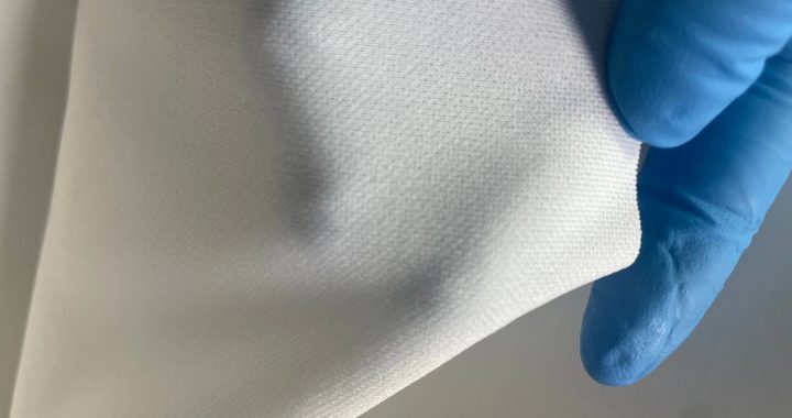
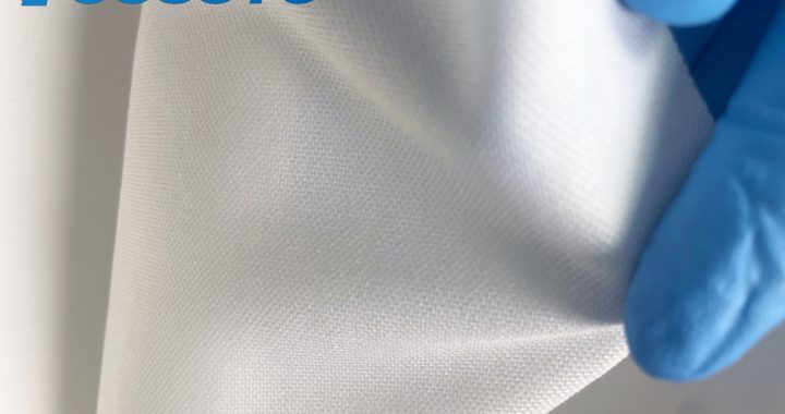
Antistatic cleanroom wipes are essential tools in protecting electronic components from damage caused by electrostatic discharge (ESD). These wipes are specifically designed to reduce static buildup, preventing costly damage during handling, assembly, and cleaning processes.

Key Features:

  • Antistatic Properties: These wipes are treated with antistatic agents that help dissipate static charges, reducing the risk of ESD and protecting sensitive electronic components.

  • Lint-Free: Designed to be lint-free, these wipes prevent the release of fibers that could contaminate delicate components and interfere with their performance.

  • Durable: Made from strong, durable materials, these wipes can be used repeatedly without tearing or losing effectiveness.

  • High Absorbency: Antistatic wipes are highly absorbent, making them ideal for cleaning dust, oils, and residues without leaving moisture behind.

Protection for Electronic Components:

  1. Prevents ESD Damage: Antistatic wipes help neutralize static charges that could potentially cause short circuits, performance issues, or irreversible damage to electronic components such as semiconductors, PCBs, and sensors.

  2. Safe for Sensitive Equipment: These wipes are non-abrasive and lint-free, making them safe to use on sensitive electronic surfaces without causing scratches or contamination.

  3. Improves Cleanliness: Using antistatic wipes ensures that electronic components are cleaned effectively without introducing additional contaminants or static charges, which is crucial for maintaining the quality and functionality of the equipment.

  4. Maintains Performance: By preventing the accumulation of dust, oils, and static, these wipes help maintain the optimal performance and longevity of electronic devices, circuit boards, and other sensitive components.

Application Range:

  • PCB Cleaning: Used in electronics manufacturing to clean printed circuit boards (PCBs) without causing static buildup or damaging the components.

  • Semiconductor Manufacturing: Essential for cleaning wafers and chips in semiconductor production to prevent ESD damage.

  • Assembly Lines: Used during the assembly of electronic devices to ensure components remain free of static charges and contaminants.

  • Final Product Wiping: Antistatic wipes are used to clean final products such as smartphones, computers, and displays before packaging, ensuring they are static-free and contamination-free.

Best Practices:

  • Single Use: Always use the wipe once and dispose of it to avoid recontamination and static buildup.

  • Store Properly: Store antistatic wipes in sealed, clean packaging to maintain their effectiveness.

  • Handle with Care: Use gloves when handling wipes to prevent introducing static or contaminants from your hands.

Application of high-density lint-free cloth in PCB cleaning

High-density cleanroom wipes are essential tools in PCB (Printed Circuit Board) cleaning, particularly in environments where precision and cleanliness are critical. Their advanced design and superior properties make them ideal for ensuring PCB surfaces are free from dust, residues, and contaminants that can interfere with the performance and reliability of electronic components.

Key Features:

  • High Fiber Density: The tightly woven fibers in high-density wipes enhance their ability to capture and retain dust, particles, and residues, improving cleaning efficiency.

  • Lint-Free: These wipes are designed to shed minimal fibers, which is critical when cleaning sensitive surfaces like PCBs, where even tiny particles can cause defects.

  • High Absorbency: Capable of absorbing liquids, oils, and flux residues effectively, these wipes help maintain dry, clean PCB surfaces.

  • Durability: The robust, high-density construction of these wipes ensures they won’t tear easily during cleaning, even in high-traffic environments.

Application Range:

  • PCB Cleaning: Ideal for cleaning the surface of PCBs during manufacturing and assembly to ensure they are free from contaminants like dust, flux, and oils.

  • Soldering Residue Removal: Used to remove solder flux residues and other contaminants after the soldering process, ensuring better connectivity and reliability.

  • Final Inspection: Wipes are used in the final inspection phase to clean PCBs before testing or packaging, ensuring no contamination affects the testing or functionality of the board.

  • Component Cleaning: Used for cleaning around delicate components on the PCB, such as resistors, capacitors, and microchips, without causing damage.

Best Practices:

  • Single Use: To avoid cross-contamination, use each wipe only once and dispose of it immediately after use.

  • Proper Storage: Keep high-density wipes in sealed, clean conditions to preserve their effectiveness and prevent exposure to contaminants.

  • Gentle Wiping: Wipe in one direction to prevent reintroducing contaminants and to achieve the best cleaning results.

  • Use with Appropriate Solvents: When needed, use the wipes with solvents like isopropyl alcohol (IPA) to effectively clean and remove residues without damaging the PCB.

Case Study: Anti-Static Wipes in Electronics Factory

Antistatic cleanroom wipes are critical in electronics manufacturing, where the cleanliness of surfaces directly impacts product performance. In this case study, we’ll explore how antistatic wipes are used effectively in electronics factories to ensure contamination control and safeguard sensitive components from electrostatic discharge (ESD).

Key Features:

  • Antistatic Properties: These wipes help neutralize static electricity, preventing ESD, which can damage sensitive electronic parts.

  • Lint-Free: Antistatic wipes are designed to be lint-free, ensuring no fiber contamination during the cleaning process.

  • Durability: Made from strong materials, they resist wear and tear, providing a long-lasting solution for cleaning tasks.

  • High Absorbency: The wipes efficiently remove oils, dust, and other contaminants without leaving moisture behind.

Application Range:

  • PCB Cleaning: Used to clean printed circuit boards (PCBs) during assembly and testing to ensure no static charge or contamination remains.

  • Semiconductor Manufacturing: These wipes are employed in semiconductor fabrication cleanrooms to maintain static-free environments.

  • Assembly Line Cleaning: Antistatic wipes are used across various workstations to keep assembly areas free of dust, oils, and static charges.

  • Final Product Wiping: They ensure that final electronic products, like smartphones and laptops, are clean, dry, and free of static charge before packaging.

Case Example:

At a leading electronics manufacturing facility, antistatic wipes are used at various stages of production. For example, during PCB assembly, workers use these wipes to clean the surface of circuit boards, ensuring no residual dust or static charge remains. Additionally, wipes are used on workbenches and equipment to prevent the buildup of static charges that could interfere with component function. Workers are trained to wipe surfaces in a single direction and immediately dispose of the wipes after use to maintain a contamination-free environment.

Best Practices:

  • Proper Storage: Store wipes in sealed, clean environments to prevent contamination or loss of antistatic properties.

  • Single Use: Dispose of wipes immediately after use to avoid cross-contamination.

  • Use in Controlled Areas: Always use antistatic wipes in static-controlled areas to maintain their effectiveness in preventing ESD.

Performance: High-Density vs. Standard-Density Wipes

High-density cleanroom wipes and regular cleanroom wipes are both essential for maintaining cleanliness in sensitive environments, but their performance differs significantly in terms of fiber structure, cleaning efficiency, and suitable applications.

Key Features:

  • Fiber Density: High-density wipes have a denser, tighter weave, offering improved strength and better particle retention compared to regular wipes.

  • Absorbency: High-density wipes absorb more liquid per square meter, making them more effective at cleaning and removing contaminants.

  • Durability: Due to their dense fiber structure, high-density wipes are more durable and resistant to wear during cleaning tasks.

  • Lint-Free: Both types are designed to be lint-free, but high-density wipes minimize shedding even more effectively.

Application Range:

  • PCB Cleaning: High-density wipes are preferred for cleaning delicate printed circuit boards (PCBs), where even minor contamination can cause damage.

  • Semiconductor Manufacturing: Used in the semiconductor industry to prevent the transfer of dust and particles onto sensitive surfaces.

  • Assembly Lines: High-density wipes are ideal for assembly stations in electronics manufacturing to maintain high levels of cleanliness.

  • Final Product Cleaning: Used in the final stages of production to clean electronic products, ensuring they are free from dust, oils, or other contaminants.

Best Practices:

  • Single Use: For optimal performance and to avoid cross-contamination, dispose of wipes after each use.

  • Proper Storage: Store wipes in sealed, clean environments to preserve their properties.

  • Unidirectional Wiping: Wipe in one direction to ensure thorough cleaning and avoid recontamination.

  • Handle with Care: Minimize handling to maintain sterility and avoid introducing contaminants.

Dust-Free Wipes for Electronics Manufacturing

Cleanroom wipes play a crucial role in electronics manufacturing by ensuring cleanliness, preventing contamination, and maintaining the integrity of sensitive electronic components.

Key Features:

  • Lint-Free: Prevents fibers from shedding, which could damage delicate components.

  • High Absorbency: Effectively absorbs oils, dust, and residues without leaving moisture behind.

  • Non-Abrasive: Cleans without causing scratches or surface damage.

  • Antistatic Properties: Helps reduce electrostatic discharge (ESD), safeguarding sensitive electronics.

Application Range:

  • PCB Cleaning: Essential for wiping printed circuit boards to avoid contamination.

  • Semiconductor Production: Ensures a contamination-free environment for semiconductor manufacturing.

  • Assembly Lines: Keeps assembly stations clean, preventing dust or fiber buildup.

  • Final Product Wiping: Used for cleaning final electronic products like monitors, phones, and other consumer electronics.

Best Practices:

  • Single Use: Wipes should be disposed of after one use to avoid cross-contamination.

  • Proper Storage: Store wipes in clean, sealed environments to maintain their lint-free and antistatic qualities.

  • Unidirectional Wiping: Clean in a single direction to prevent recontamination.

  • Handle with Care: Avoid touching the wipe surface directly to maintain its sterility.

PCB Cleaning with Pre-Moistened Wipes

Pre-wetted cleanroom wipes offer an efficient solution for cleaning PCBs, ensuring a dust-free and residue-free surface while preserving sensitive components.

Key Features:

  1. Optimal Moisture: Pre-wetted wipes provide consistent moisture, ideal for cleaning PCBs without excess liquid.

  2. Lint-Free: Prevents fibers and particles from contaminating PCB surfaces, ensuring high-quality assembly.

  3. Strong Absorbency: Effectively removes dust, oils, and flux residues without leaving behind any contaminants.

  4. Non-Abrasive: Safe for delicate components, reducing the risk of scratches or physical damage.

Application Range:

  • PCB Assembly: Ideal for cleaning PCBs during the assembly process to prevent contamination.

  • Soldering and Flux Removal: Helps clean flux residues and other contaminants after soldering.

  • Pre-Cleaning: Prepares PCB surfaces for further processes such as testing or coating.

  • Surface Preparation: Used before applying adhesives, coatings, or during other finishing processes.

Best Practices:

  • Gentle Wiping: Use gentle, unidirectional strokes to avoid re-contaminating cleaned areas.

  • Single-Use Only: Discard wipes after use to avoid cross-contamination.

  • Proper Storage: Store wipes in sealed packaging to maintain cleanliness and prevent drying out.

  • Inspect Surface: Always check the PCB surface for any remaining residue or contamination after cleaning.

Benefits:

  • Prevents Contamination: Ensures PCBs are free of dust, oils, and other contaminants that could affect performance.

  • Enhances Assembly Quality: Lint-free wipes ensure no particles interfere with delicate components or circuits.

  • Improves Efficiency: Pre-wetted wipes save time by providing an effective and quick cleaning solution.

  • Protects Sensitive Components: Non-abrasive design ensures PCBs remain undamaged during cleaning.

Advantages of high-density, lint-free wipes in PCB cleaning

High-density cleanroom wipes are ideal for cleaning printed circuit boards (PCBs), providing superior particle removal and liquid absorption while protecting delicate electronic components. Their advanced fiber structure ensures efficient, residue-free cleaning in sensitive environments.

Key Features:

  1. High-Density Fiber Structure: Tightly woven fibers increase surface contact and enhance the ability to capture dust, oils, and residues.

  2. Enhanced Absorbency: Can hold more cleaning solutions like IPA, ensuring thorough cleaning with fewer wipes.

  3. Lint-Free and Non-Abrasive: Prevents fiber shedding and scratches on sensitive PCB surfaces, protecting component integrity.

  4. Chemical Compatibility: Resistant to solvents such as IPA and deionized water, allowing safe cleaning of boards and components.

Applications:

  • PCB Manufacturing: Removes residues and particles during assembly and inspection.

  • Electronics Repair: Cleans circuit boards without damaging components or conductive paths.

  • Semiconductor Equipment: Maintains cleanliness of tools and fixtures used in PCB processing.

  • Cleanroom Maintenance: Supports Class 100–1000 cleanroom standards during routine cleaning tasks.

Benefits:

  • Improved Cleaning Efficiency: High-density design reduces the number of wipes needed.

  • Protects Sensitive Components: Non-abrasive, lint-free material ensures PCBs remain undamaged.

  • Reduces Contamination Risk: Captures more dust and liquids, maintaining high-quality electronics production.

PCB Cleanroom Wipes: Selection & Use Guide

In the precision-demanding fields of PCB manufacturing and electronics, the choice of cleanroom wipes directly influences product quality and production environment cleanliness. This guide provides an in-depth overview of how to select and properly use cleanroom wipes specifically for PCB circuit board cleaning, covering material selection, edge finishing, size, cleanliness level, and practical usage tips.

1. Cleanroom Wipe Selection Guide

Material Selection:

  • Polyester Fiber: Most standard cleanroom wipes use 100% polyester double-knit fabric. This material offers a soft surface with low fiber shedding due to friction, suitable for general PCB cleaning tasks.

  • Ultrafine Fiber: Made from 80% polyester and 20% nylon blend, ultrafine wipes provide superior liquid absorption and are ideal for precision cleaning tasks such as chips and microprocessors, effectively removing fine particles.

Edge Finishing:

  • Laser Edge Sealing: Uses high-temperature fusion to melt fibers, reducing lint generation. Edges are relatively rigid but ensure high cleanliness, fitting most PCB cleaning scenarios.

  • Ultrasonic Edge Sealing: Offers softer edges, better for highly sensitive surfaces like optical components, though at a higher cost.

  • Avoid Raw Cut Edges: Unsealed wipes tend to shed lint, posing risk of secondary contamination.

Basis Weight and Size:

  • Basis Weight: Polyester wipes with ≥120g/m² balance absorption and durability. Ultrafine wipes with ≥120g/m² are also recommended for enhanced performance.

  • Size: Common sizes include 4″×4″, 6″×6″, and 9″×9″. Larger wipes (9″) suit broad surface cleaning, while smaller sizes are better for delicate or confined areas. The 9″ size is widely used.

Cleanliness Grade:

  • Choose wipes based on the production environment’s cleanroom class. For example, Class 100 cleanrooms require Class 100 cleanroom wipes.

Additional Features:

  • Anti-Static: Wipes with anti-static properties (often achieved via conductive fibers) prevent static buildup and dust attraction, safeguarding PCB performance. For less stringent needs, solvent-wetting can reduce static.

  • Pre-Wetted Options: Some wipes come pre-impregnated with alcohol (e.g., IPA), reducing on-site spraying. More common internationally than domestically.

2. Proper Usage of Cleanroom Wipes

Pre-Wetting:

  • Use high-purity solvents such as ≥99% isopropyl alcohol (IPA) or ethanol.

  • Ensure uniform wetting via controlled soaking devices to avoid overly wet or dry spots.

Unpacking Procedures:

  • Perform unpacking in Class 1000 or higher cleanroom environments, wearing cleanroom garments, gloves, and masks.

  • Wipe the outer packaging opening with a cleanroom wipe moistened with solvent to prevent external contamination.

Wiping Techniques:

  • Fold wipes to enclose edges internally, preventing lint from edges contacting PCB surfaces—especially important for ultrasonic sealed wipes which can be abrasive.

  • Use unidirectional wiping with light, consistent pressure to avoid redeposition of particles or surface scratching.

  • Adjust wiping force according to PCB surface sensitivity, with extra care on pads or sensitive areas.

Solvent Use:

  • Apply enough solvent to moisten the wipe without dripping to avoid residue from evaporation.

  • Test new solvents on small PCB areas first to confirm compatibility and avoid corrosion.

Storage and Reuse:

  • Seal unused wipes immediately to prevent dust absorption.

  • High-end wipes may be reused after cleaning with ultrapure water (18 MΩ·cm) and drying in a cleanroom; ordinary wipes are generally single-use.

3. Important Precautions

  • Wear anti-static wristbands and ensure grounded workstations to prevent ESD damage to components.

  • Avoid wiping multiple areas with the same wipe to reduce cross-contamination risks.

  • Regularly monitor cleanroom temperature and humidity.

4. Recommended Brands and Models

  • Brands: Preferably YUSTER (domestic) or TEXWIPE (international).

  • Models:

    • K122 Series: 120g basis weight, laser or ultrasonic sealed edges, suitable for PCB boards and applications involving liquids. Available in four sizes.

    • K610 Series: 180g basis weight ultrafine fiber with laser or ultrasonic sealing, excellent absorption for high-precision cleaning.

Summary

For budget-conscious scenarios, 120g laser-cut polyester wipes provide reliable cleaning. For higher requirements and budgets, 180g laser-cut ultrafine fiber wipes offer enhanced absorption and gentler cleaning for delicate PCB surfaces.

SMT Stencil Wipes: Essential for Electronics

In surface mount technology (SMT) production, the solder stencil is a core tool enabling precise solder paste printing. However, residues such as solder paste and red glue around the stencil apertures directly affect print quality, leading to defects like solder balls and bridging. SMT solder stencil cleaning wipes, as a key consumable for stencil cleaning, play a critical role in ensuring electronic product yield and reliability. This article analyzes their material characteristics, application scenarios, and industry development trends to highlight their core industrial value.

  1. Definition and Core Functions of SMT Solder Stencil Cleaning Wipes
    SMT solder stencil cleaning wipes are dust-free wiping materials designed specifically for SMT printers to remove excess solder paste, red glue, and other contaminants from the stencil underside and printed circuit boards (PCBs). Their main functions include:

  • High-efficiency cleaning: Physically adsorbing and chemically dissolving micron-level residues to prevent contamination of stencil apertures.

  • Defect prevention: Reducing defects like shorts and missing prints in the solder paste printing process to improve PCB yield.

  • Compatibility: Suitable for various SMT printers (e.g., DEK, MPM, EKRA) to meet diverse machine cleaning requirements.

Industry statistics indicate that about 50% of SMT final defects originate from the stencil printing process. Using high-quality wipes, such as those produced by Uster — a leading domestic manufacturer offering free samples and a full range of specifications compatible with common printer brands like DEK, MPM, Panasonic, and Sony — can significantly reduce such defects. Custom non-standard sizes are also supported.

  1. Material Characteristics and Performance Requirements
    SMT solder stencil wipes must meet strict standards for cleanliness, durability, and functionality. Typical material features include:

  • Dual-layer composite structure:

    • Wood pulp layer (textured side): Made from natural wood pulp fibers, soft and highly absorbent to conform to the stencil surface without scratching and capture dust.

    • Polyester layer (smooth side): Made of polyester fibers, wear-resistant with a “sieve effect” to reduce fiber shedding and prevent contamination of solder paste.

  • Spunlace technology: The wood pulp and polyester fibers are bonded via spunlace, creating a strong, low-lint nonwoven fabric.

  • Solvent compatibility: Wipes must be compatible with common cleaning solvents such as isopropanol (IPA) and alcohol to ensure rapid absorption and uniform distribution without chemical degradation or contamination.

  • Anti-static and low VOC design:

    • Anti-static treatment reduces dust attraction, crucial for high-precision electronics manufacturing.

    • Pre-saturated wipes reduce VOC emissions, protecting operator health and workplace safety.

  • Emerging material innovations:
    Future wipes may incorporate new materials such as polyester-wood pulp blends for faster absorption and durability, ultra-fine fibers for high-density circuits, or resin-bonded materials to enhance adhesion and cleaning effectiveness.

  1. Application Scenarios and Operation Guidelines
    SMT solder stencil wipes are widely used in:

  • Printer cleaning:

    • Manual/semi-automatic printers: Regular wiping of stencil undersides to prevent solder paste buildup.

    • Fully automatic printers: Integrated in automated cleaning systems for continuous production efficiency (e.g., DEK, MPM).

  • Abnormal handling:

    • Misprint repair: Quickly removing thick glue or partially cured epoxy with pre-saturated wipes.

    • Extreme contamination: Using high-absorbency foam wipes for stubborn residues on metal screens or thick-film prints.

  • Proper usage steps:

    • Differentiate wipe sides: The textured (wood pulp) side contacts the stencil, while the smooth (polyester) side contacts the cleaning solvent.

    • Spray solvent on the smooth side for even distribution.

    • Apply light pressure and wipe in a single direction to avoid re-contamination.

  1. Industry Trends and Future Directions

  • Environmental sustainability:

    • Reducing industrial waste and energy consumption.

    • Uster’s efforts in minimizing raw material waste through size optimization and deploying advanced production lines to maximize energy efficiency.

  • Smart customization:

    • Offering custom wipe widths and lengths tailored to printer models (e.g., Panasonic, Yamaha) and PCB sizes.

    • Developing intelligent monitoring systems to track wipe cleaning effectiveness and wear status in real-time.

  • Growth of high-end niche markets:

    • Formulating products dedicated to high-end and specialized SMT applications.

  1. Conclusion
    Though SMT solder stencil cleaning wipes may be considered a “hidden consumable,” their impact on product quality and manufacturing efficiency is undeniable. As SMT technology evolves toward higher density and speed, innovations in wipe materials and manufacturing processes will continue to drive industry advancement. Selecting wipes that meet specific production needs is key to reducing defects, promoting green manufacturing, and facilitating intelligent transformation.

Wiepstar SMT Wipes: Precision Manufacturing Guardians

In modern electronics manufacturing, the accuracy and stability of Surface Mount Technology (SMT) processes directly affect the quality and reliability of final products. As an essential consumable in the SMT production line, Wiepstar’s SMT stencil cleaning wipes have become the trusted “invisible quality gatekeeper” for PCB (Printed Circuit Board) manufacturers worldwide, providing solid support for cleaning and quality assurance in precision manufacturing.

1. Core Advantages of Wiepstar SMT Stencil Cleaning Wipes

  • Perfect Combination of Natural Materials and Advanced Processing
    Wiepstar uses premium natural wood pulp and high-quality raw materials, processed through a unique spunlace technology to create a dual-layer structure of wood pulp and polyester. This design ensures the wipes are flexible and durable while offering excellent absorption capabilities to effectively remove solder paste residues, oils, and micron-level particles, avoiding secondary contamination from fiber shedding on sensitive electronic components.

  • Outstanding Cleaning Performance Ensures Printing Quality

    • High absorbency and low lint generation efficiently remove solder paste residues and adhesives, reducing defects such as solder bridges and insufficient solder joints.

    • Leaves the PCB surface smooth and scratch-free after wiping, ensuring precise solder paste transfer and stable solder joints.

    • Maintains strength under intense use, significantly extending service life and reducing replacement frequency and costs.

  • Comprehensive Compatibility and Adaptability
    Wiepstar’s SMT wipes come in a full range of specifications covering most major SMT printing machine brands (such as MPM, DEK, YAMAHA) and support custom non-standard sizes to meet diverse production needs. Their unique porous structure is highly compatible with the vacuum systems of stencil printers, enhancing solder paste removal efficiency and maintaining production speed.

  • Cost Savings and Efficiency Gains
    By reducing cleaning time, solvent consumption, and defect rates, Wiepstar helps manufacturers significantly lower production costs. The wipes’ high cleaning efficiency accelerates production throughput and improves capacity and delivery performance, boosting competitiveness.

2. Wide Application Areas

  • Consumer Electronics Production Lines: Support high-frequency cleaning in flagship smartphone production to ensure solder joint accuracy and product stability.

  • Automotive Electronics Workshops: Provide reliable cleaning performance in harsh vibration environments, safeguarding critical components such as vehicle control units.

  • Aerospace Industry: Meet the zero-defect standards required for circuit boards in space-grade products operating under extreme conditions.

  • Research and Laboratory: Offer dust-free and lint-free cleaning solutions for precision instruments and scanning electron microscopes.

3. Why Choose Wiepstar?

As a professional domestic manufacturer of SMT stencil cleaning wipes, Wiepstar adheres to a “source quality” principle, strictly controlling every stage from raw material selection to production processes to ensure products meet international cleanliness and performance standards. The company offers free samples for trial, ready stock supply, and OEM/ODM customization services to meet varied client requirements. Whether you are a contract manufacturer pursuing maximum efficiency or a high-end manufacturer focused on quality assurance, Wiepstar provides reliable, customized cleaning solutions you can trust.