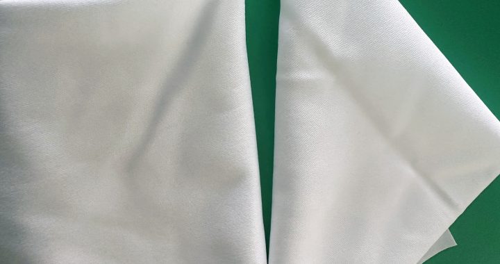
Printed Circuit Boards (PCBs) in laboratory settings—used for sensor arrays, testing equipment, or prototype electronics—require meticulous cleaning to remove flux residues, solder debris, and dust. Even minor contamination can cause signal interference, short circuits, or component failure. High-density cleanroom wipes, with their thick, tightly woven structures and ultra-low linting properties, outperform standard wipes in PCB cleaning. Below are their key advantages, tailored to the unique demands of lab-based PCB maintenance and testing.
1. Superior Particle and Residue Trapping: Eliminates Microscopic Contaminants
Lab PCBs often feature fine-pitch components (0.4mm or smaller) and sensitive traces, where sub-micron particles or leftover flux can disrupt functionality. High-density wipes excel here by:
- Dense Capillary Networks: Their tight weave (250–400 gsm) creates millions of tiny channels that trap particles as small as 0.05μm—far smaller than the 0.5μm particles standard wipes miss. This is critical for cleaning around SMDs (Surface-Mount Devices) or BGA (Ball Grid Array) packages, where dust can lodge between pins and cause connectivity issues.
- Effective Flux Dissolution: When paired with high-purity solvents (e.g., 99% IPA), the thick, absorbent fibers of high-density wipes hold solvent longer, allowing it to fully dissolve rosin or no-clean flux residues. Unlike thin wipes that dry out quickly, high-density variants require fewer passes to remove stubborn flux—reducing the risk of scrubbing that can damage PCB traces.
- Ultra-Low Linting: Made from continuous-filament polyester or microfiber, these wipes shed ≤1 fiber per use. This eliminates fiber contamination, a major cause of short circuits in lab PCBs (where even a single 1μm fiber can bridge adjacent traces).
2. Durability for Precision Handling: Avoids In-Use Damage
Lab PCBs are often prototypes or low-volume units, making damage during cleaning costly. High-density wipes protect PCBs by:
- Tear and Fray Resistance: Reinforced, heat-sealed edges prevent fraying, even when wiping around sharp component leads or PCB edges. Standard wipes often tear during this process, leaving loose fibers or fragmented wipe material on the board.
- Abrasion Protection: Their soft, plush texture glides over PCB surfaces without scratching solder masks or delicate component coatings (e.g., gold-plated pins). This is especially important for lab PCBs with exposed copper traces or optical sensors mounted directly on the board.
- Reusable (When Approved): For non-critical lab PCBs (e.g., test fixtures), high-density wipes can be rinsed with solvent and reused, reducing waste. Their durable structure maintains performance through 3–5 uses, unlike standard wipes that degrade after a single pass.
3. Controlled Liquid Absorption: Prevents Solvent Damage
Over-saturating PCBs with solvent can seep into components (e.g., capacitors, ICs) and cause internal damage. High-density wipes address this by:
- Uniform Solvent Retention: They absorb 10–15x their weight in solvent (e.g., IPA) and release it evenly, preventing drips or pooling on the PCB. This ensures consistent cleaning without risking solvent intrusion into component housings.
- Fast, Streak-Free Drying: The dense fibers distribute solvent across the PCB surface, promoting rapid, even evaporation. This eliminates solvent streaks or residues that can attract dust later, reducing the need for re-cleaning.
- Compatibility with Specialty Solvents: High-density wipes resist degradation from harsh PCB cleaning solvents (e.g., flux removers, acetone) that would break down standard wipes. This allows labs to use the most effective solvent for the job without compromising wipe performance.
4. Consistency for Lab Quality Control
Laboratory work demands repeatable results, and cleaning consistency is critical for reliable PCB testing. High-density wipes deliver this by:
- Uniform Performance: Each wipe has the same thickness, fiber density, and absorption capacity, ensuring every PCB receives the same level of cleaning. This eliminates variability from standard wipes, which can have inconsistent fiber distribution.
- Compliance with Lab Standards: Many high-density wipes meet ISO 14644-1 Class 5 standards and IPC-A-610 (electronics assembly guidelines), aligning with lab quality control requirements. This is essential for labs conducting regulated testing (e.g., aerospace or medical PCB validation).
For laboratories relying on PCBs for accurate testing or prototyping, high-density cleanroom wipes are a strategic choice—they protect delicate components, eliminate microscopic contamination, and ensure consistent cleaning results that support reliable lab work.
