Class 100 cleanrooms (ISO Class 3)—critical for semiconductor wafer fabrication, microelectronics assembly, and precision optics manufacturing—require ultra-stringent contamination control (≤100 particles ≥0.5μm per cubic foot). Even minor electrostatic discharge (ESD) or fiber debris can ruin high-value products (e.g., 3nm wafers) or damage sensitive equipment. Anti-static cleanroom wipes are foundational to these workflows, but optimizing their selection, usage, and integration into cleaning protocols is key to maximizing efficiency and minimizing risks. Below is a detailed guide to optimizing their role in Class 100 cleanroom processes.
1. Wipe Selection Optimization: Match to Cleanroom Tasks & Materials
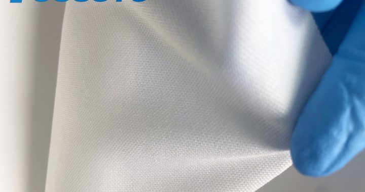
The first step in optimization is selecting anti-static wipes tailored to Class 100 requirements—generic wipes often fail to meet particle, ESD, or purity standards:
- Material & Linting Control:
- Use continuous-filament polyester or ultra-fine microfiber wipes (0.1μm fiber diameter) to ensure linting ≤1 fiber (≥0.1μm) per use—compliant with ISO Class 3 standards. Avoid staple-fiber wipes (e.g., cotton blends), which shed 5–10x more fibers and introduce particulate contamination.
- For solvent-based cleaning (e.g., flux removal, wafer edge cleaning), choose solvent-resistant anti-static wipes (e.g., polyester with epoxy bindings) that retain structure when exposed to 99.9% IPA or acetone—preventing fiber breakdown and residue leaching.
- ESD Performance:
- Select wipes with surface resistance 10⁶–10¹⁰ Ω (ANSI/ESD S20.20 compliant) for most tasks—this range balances fast charge dissipation (prevents dust attraction) and safety (avoids electrical shorts on wafers). For high-risk areas (e.g., EUV lithography tools), use conductive wipes (10³–10⁶ Ω) for immediate charge neutralization.
- Size & Format:
- Opt for 4”x4” or 6”x6” wipes for precision tasks (e.g., cleaning wafer chucks, reticles) to minimize over-wiping and solvent contact with critical surfaces. Use perforated rolls for large-area cleaning (e.g., equipment exteriors) to reduce waste—tear off only the size needed.
2. Cleaning Process Optimization: Streamline Workflows & Reduce Risk
Integrating anti-static wipes into standardized, step-by-step processes eliminates variability and reduces contamination events:
A. Wafer Handling Area Cleaning (Pre/Post-Processing)
- Pre-Processing (Before Wafer Loading):
- Use a dry anti-static wipe to dust wafer cassettes, vacuum chuck surfaces, and load-port doors—focus on crevices where particles accumulate (e.g., cassette slots). Fold the wipe into a thin strip to reach tight gaps.
- Follow with a pre-wet anti-static wipe (99.9% electronic-grade IPA) to clean chuck surfaces—wipe in a single circular motion (1 full rotation) with light pressure (<0.5 psi) to avoid scratching the chuck’s ceramic coating.
- Dispose of wipes immediately after use—do not reuse on multiple cassettes/chucks.
- Post-Processing (After Wafer Unloading):
- Use a fresh dry anti-static wipe to remove residual wafer dust from cassettes.
- Sanitize load-port doors with a pre-wet wipe to remove organic residues (e.g., from wafer tape)—this prevents cross-contamination between batches.
B. Optics Maintenance (Lithography Tools, Metrology Equipment)
- 1. Pre-Clean Prep:
- Power down the tool, purge the optic chamber with nitrogen, and wear Class 10 cleanroom gloves to avoid skin oil transfer.
- 2. Dust Removal:
- Use a dry anti-static microfiber wipe to gently blot (not wipe) optic surfaces (e.g., reticles, EUV lenses)—blotting minimizes friction and avoids scratching AR coatings.
- 3. Residue Cleaning (If Needed):
- For organic residues, use a pre-wet anti-static wipe (lens-grade IPA) in a single linear stroke (from edge to edge)—dispose of the wipe after one stroke to prevent re-depositing particles.
- 4. Final Inspection:
- Check optics with a particle counter (target: 0 particles ≥0.1μm) before reassembling the tool.
C. Daily Equipment Sanitization
- Frequency: Clean all equipment surfaces (e.g., tool exteriors, workbenches, cart handles) every 4 hours to prevent dust buildup.
- Process:
- Use a dry anti-static wipe to remove loose dust.
- Follow with a pre-wet anti-static wipe (70% IPA) to sanitize and remove remaining particles—wipe in overlapping horizontal strokes to ensure full coverage.
- Log each cleaning event in the cleanroom’s maintenance record to track compliance.
3. Waste & Cost Optimization: Minimize Usage Without Compromising Quality
Class 100 cleanrooms often overuse wipes due to poor process design—optimization reduces waste while maintaining cleanliness:
- Wipe Segmentation: Fold wipes into 4–6 usable quadrants; use one quadrant per task section (e.g., one quadrant for a wafer cassette slot, another for the chuck). This extends wipe life by 3–4x.
- Solvent Efficiency: Use pre-wet wipes instead of “dry wipe + bulk solvent”—pre-wet wipes contain pre-measured solvent, reducing waste by 50% (bulk solvent often over-saturates wipes, leading to drips and excess usage).
- Inventory Management: Track wipe usage per task (e.g., 1 wipe per wafer cassette) to set par levels—avoid overstocking (wipes degrade over time in cleanrooms) or stockouts (causes process delays).
4. Validation & Continuous Improvement
- Particle Count Monitoring: Measure surface particle levels (using a portable particle counter) before and after cleaning—ensure post-clean levels meet ISO Class 3 standards (≤10 particles ≥0.1μm per square foot).
- ESD Testing: Monthly test anti-static wipes’ surface resistance (using an ESD meter) to confirm they maintain 10⁶–10¹⁰ Ω—replace wipes if resistance drifts outside this range.
- Worker Training: Train cleanroom staff on optimized wipe usage (e.g., folding techniques, stroke direction) and conduct quarterly refresher courses—variability in human behavior is a top cause of cleaning failures.
By optimizing anti-static wipe selection, processes, and waste management, Class 100 cleanrooms reduce contamination events by 40–50%, cut wipe costs by 30%, and extend equipment lifespan—critical for manufacturing high-precision, high-value products.