Anti-Static Wipes in Semiconductor Cleanroom Cleaning

Semiconductor cleanrooms (ISO Class 1–5) operate in an ultra-sensitive environment where even sub-micron particles or electrostatic discharge (ESD) can ruin 3nm–7nm wafers, damage lithography tools, or halt production lines. Anti-static cleanroom wipes—engineered with static-dissipative materials and ultra-low linting properties—are a cornerstone of contamination control here, addressing both particle buildup and ESD risks that generic wipes cannot. Below is a detailed breakdown of their critical applications across semiconductor cleanroom workflows, from wafer handling to equipment maintenance.

1. Wafer Surface Cleaning: Protecting Critical Substrates

Wafers are the core of semiconductor manufacturing, and their surfaces must remain free of particles, oils, and static to ensure successful etching, deposition, and packaging. Anti-static wipes play a pivotal role in:
  • Pre-Process Wafer Cleaning: Before lithography or thin-film deposition, anti-static dry wipes (surface resistance: 10⁶–10¹¹ Ω, per ANSI/ESD S20.20) gently remove ambient dust from wafer backsides and edges. The wipes’ continuous-filament polyester construction traps particles as small as 0.05μm without scratching the wafer’s delicate oxide layer.
  • Post-Soldering Residue Removal: For wafer-level packaging (WLP), pre-moistened anti-static wipes (impregnated with 99.9% high-purity IPA) dissolve flux residues and solder splatters from bond pads. The static-dissipative material prevents charge buildup that could attract floating particles to the wafer’s active areas.
  • Edge Bead Cleaning: Wafers often have “edge beads” (excess photoresist) along their rims. Anti-static wipes, folded into narrow strips, target these beads without contacting the wafer’s central processing area—ensuring no residue or fibers interfere with pattern transfer.

2. Equipment Maintenance: Safeguarding High-Value Tools

Semiconductor tools like lithography scanners, wafer chucks, and transfer robots require regular cleaning to maintain precision. Anti-static wipes protect these tools by:
  • Lithography Tool Optics Cleaning: The laser lenses and reticle masks in lithography tools are prone to static-attracted dust, which distorts light patterns and causes print defects. Anti-static pre-wet wipes (with deionized water + 5% IPA) clean these optics without generating static, while their low-linting design avoids fiber deposits on lens surfaces.
  • Wafer Chuck Decontamination: Wafer chucks use vacuum suction to hold wafers during processing, and residue buildup here causes wafer misalignment. Anti-static dry wipes remove dust and oxide films from chuck grooves, while their static-dissipative properties prevent the chuck from attracting new particles post-cleaning.
  • Transfer Robot Arm Cleaning: Robot arms that move wafers between tools accumulate silicon dust and lubricant residues. Anti-static wipes (resistant to mild solvents) clean arm grippers and rails, ensuring smooth, particle-free wafer handling—critical for avoiding wafer scratches or drops.

3. Workbench and Surface Sanitization: Controlling Cross-Contamination

Semiconductor cleanroom workbenches, fume hoods, and storage surfaces are common sources of particle and static transfer. Anti-static wipes address this by:
  • Daily Workbench Cleaning: Technicians use anti-static dry wipes to dust workbenches before and after wafer handling. The wipes’ static-dissipative properties neutralize charge on the bench surface, preventing it from attracting dust that could transfer to wafers.
  • Spill Response for Solvents: Accidental spills of IPA or photoresist require fast, safe cleanup. Anti-static pre-wet wipes (chemically compatible with semiconductor solvents) absorb spills without generating static, while their high density prevents solvent breakthrough that could damage bench underlayers.
  • Storage Container Cleaning: Wafer cassettes and transport containers are cleaned with anti-static wipes to remove dust and static before loading wafers. This ensures no contaminants are introduced during wafer storage or transport between cleanroom bays.

4. ESD-Sensitive Component Handling: Protecting ICs and Sensors

Semiconductor cleanrooms also assemble ESD-sensitive components like IC chips, sensors, and microcontrollers. Anti-static wipes support this by:
  • Component Lead Cleaning: IC chip leads are prone to oxidation and oil buildup, which disrupt solder joints. Anti-static pre-wet wipes (70% IPA) clean leads without generating static, ensuring reliable electrical contact during assembly.
  • Sensor Surface Protection: MEMS sensors and image sensors have ultra-delicate surfaces that static can damage. Anti-static dry wipes gently remove dust from these components, while their soft texture avoids scratching sensor diaphragms or pixel arrays.

Key Benefits of Anti-Static Wipes in Semiconductor Cleanrooms

  • Defect Reduction: By eliminating static and particles, anti-static wipes reduce wafer defects by 40–60% compared to generic wipes.
  • Tool Longevity: Gentle, static-free cleaning extends the lifespan of lithography tools, chucks, and robots by 2–3 years.
  • Compliance Assurance: Wipes meet ISO 14644-1 Class 1–5 standards and SEMI F21 guidelines, ensuring adherence to semiconductor industry regulations.
In semiconductor cleanrooms, where precision and contamination control are non-negotiable, anti-static cleanroom wipes are more than a cleaning tool—they are a critical enabler of high-yield, reliable chip manufacturing.
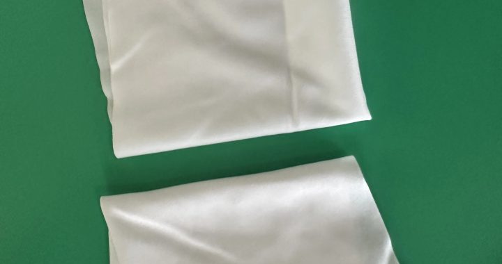
Cleaning Wipes in Semiconductor Equipment Maintenance

Semiconductor cleanrooms (ISO Class 1–5) rely on ultra-precise equipment—lithography tools, wafer chucks, transfer robots, and metrology systems—to fabricate 3nm–7nm chips. Even sub-micron particles, flux residues, or electrostatic discharge (ESD) during maintenance can ruin wafers, damage sensors, or halt production. Specialized semiconductor cleaning wipes—engineered for low linting, ESD safety, and residue-free performance—have become indispensable for equipment upkeep, replacing risky manual solvent application or generic wipes. Below is a detailed breakdown of their applications in critical maintenance tasks, along with how they protect high-value semiconductor equipment.

1. Routine Surface Cleaning: Preventing Particle Buildup

Daily use causes dust, lint, and wafer fragments to accumulate on equipment exteriors and contact surfaces—left unchecked, these particles transfer to wafers or clog mechanical parts. Cleaning wipes address this through:
  • Sub-Micron Particle Trapping: Wipes made from ultra-fine microfiber (0.1μm diameter) or continuous-filament polyester trap particles as small as 0.05μm, far below the ISO Class 1 limit of 1 particle (≥0.1μm) per cubic foot. For transfer robot arms (a common particle hotspot), wipes remove debris from grippers and rails, preventing wafer scratches during handling.
  • ESD-Safe Formulations: Anti-static cleaning wipes (surface resistance: 10⁶–10¹¹ Ω, per ANSI/ESD S20.20) dissipate static while cleaning, avoiding charge buildup that attracts floating particles. This is critical for lithography tool exteriors, where static can pull dust onto lens covers and distort light patterns.
  • Non-Abrasive Action: The soft wipe texture cleans anodized aluminum housings, plastic control panels, and stainless steel surfaces without scratching—unlike paper towels or abrasive cloths that damage protective coatings.

2. Precision Component Maintenance: Residue Removal

Semiconductor equipment components (e.g., wafer chucks, connector pins) often accumulate flux residues (from soldering) or ionic contaminants (from cleaning solvents) that degrade performance. Cleaning wipes target these residues:
  • Wafer Chuck Cleaning: Pre-wet wipes with 99.9% high-purity IPA dissolve organic residues and oxide films on chuck surfaces. The wipes’ lint-free design ensures no fibers remain in chuck grooves—residues or fibers here cause wafer misalignment, leading to print defects in lithography.
  • Connector Pin Care: Gold-plated connector pins (used in metrology systems) are prone to oxidation and oil buildup. Cleaning wipes with mild, non-corrosive solvents remove contaminants without damaging the gold coating, ensuring reliable electrical signal transmission for accurate wafer measurements.
  • Lens and Optic Maintenance: Lithography tool optics (e.g., laser mirrors, reticle masks) require streak-free cleaning. Pre-wet wipes with deionized water + 5% IPA evaporate completely, leaving no residues that could scatter laser light or reduce image sharpness.

3. Post-Maintenance Sanitization: Avoiding Cross-Contamination

After repairing equipment (e.g., replacing a sensor in a wafer handler), cleaning wipes sanitize surfaces to prevent introducing external contaminants into the cleanroom:
  • Residue-Free Disinfection: Wipes formulated with hydrogen peroxide (3%) or peracetic acid sanitize tool interiors without leaving toxic residues. This is critical for equipment like wet process stations, where biological or chemical contaminants can contaminate wafer baths.
  • Seam and Crevice Cleaning: Wipes can be folded into narrow strips to reach tight spaces (e.g., between equipment panels, around valve controls) where dust or cleaning fluids collect during repairs. This ensures no hidden contaminants are left to migrate to wafers during operation.

4. Emergency Spill Response: Minimizing Downtime

Accidental spills of solvents (e.g., IPA, acetone) or process fluids (e.g., photoresist) on equipment require fast, safe cleanup to avoid corrosion or electrical damage. Cleaning wipes enable rapid response:
  • High Absorbency: High-density cleaning wipes absorb up to 15x their weight in liquids, containing spills before they seep into equipment casings or reach electrical components. For example, wiping up an IPA spill on a transfer robot’s circuit board prevents short circuits and costly repairs.
  • Chemical Compatibility: Wipes resistant to harsh solvents (e.g., acetone, NMP) avoid disintegrating during cleanup, ensuring no fiber fragments mix with the spill and contaminate the cleanroom.

5. Compliance and Traceability: Meeting Semiconductor Standards

Semiconductor manufacturing requires strict adherence to standards like SEMI F21 (equipment cleaning) and ISO 14644-1. Cleaning wipes support compliance by:
  • Certified Purity: Wipes meet ISO Class 1–5 particle limits and are tested for extractables (e.g., ions, metals) to ensure they do not introduce contaminants. Manufacturers provide Certificates of Analysis (CoAs) for each batch, enabling traceability.
  • Minimized Waste: Single-use, pre-portioned wipes reduce solvent waste compared to manual spraying, aligning with sustainability goals while ensuring consistent cleaning efficacy.
In semiconductor cleanrooms, cleaning wipes are more than a maintenance tool—they are a critical component of quality control, protecting equipment integrity, reducing downtime, and ensuring the production of defect-free chips.