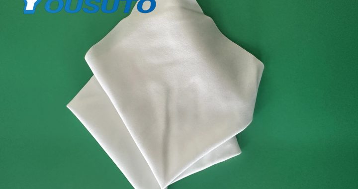
PCB solder areas—including solder joints, component leads, and pad surfaces—are prone to flux residues, rosin deposits, and handling oils that impair electrical conductivity, cause corrosion, or disrupt subsequent assembly steps. IPA (Isopropyl Alcohol) wipes are the gold standard for this cleaning task, but unstructured processes lead to inefficiency, residue left behind, or damage to delicate components. Below is an optimized, step-by-step workflow to enhance cleaning speed, consistency, and safety for PCB solder areas.
1. Pre-Clean Preparation: Set the Stage for Efficiency & Safety
Proper prep eliminates rework, prevents ESD damage, and ensures IPA wipes target only solder areas:
- PCB & Workspace Prep:
- Cool the PCB: Wait for solder areas to cool to <40°C (104°F) post-welding—hot surfaces evaporate IPA instantly, leaving residue and increasing fire risk.
- Ground & Secure: Place the PCB on an ESD-safe mat and secure it with non-abrasive clips (to avoid shifting during cleaning). Wear an ESD wrist strap (tested to 10⁶–10⁹ Ω) to protect ESD-sensitive components (e.g., microchips near solder joints).
- Mask Non-Solder Areas: Use low-tack, ESD-safe tape to cover connectors, IC sockets, or exposed circuits adjacent to solder areas—prevents IPA from seeping into these components and causing short circuits.
- IPA Wipe Selection:
- For Flux Residues: Choose 99% electronic-grade IPA wipes (low impurities ≤10 ppb) with lint-free, continuous-filament polyester fibers—high-purity IPA dissolves rosin/flux quickly, while polyester resists disintegration from solvent exposure.
- For Delicate Solder Joints (e.g., 0.4mm Fine-Pitch): Opt for mini IPA wipes (2”x2”) or cut standard wipes into 1cm-wide strips—precision ensures the wipe only contacts the solder area, not fragile component leads.
- Avoid Low-Quality Wipes: Steer clear of staple-fiber or fragrance-added wipes—they shed fibers that clog solder joints and leave sticky residues.
2. Step 1: Loosen Heavy Flux Residue (For Post-Rework Solder Areas)
For thick, dried flux (common after reflow soldering or rework), pre-treat to reduce scrubbing and component damage:
- Tear a small section of the IPA wipe and lightly dampen the solder area—do not saturate (excess IPA spreads to masked areas).
- Hold the damp wipe against the residue for 3–5 seconds to let IPA penetrate and soften the flux—this cuts cleaning time by 40% and avoids pressing residue into solder pads.
- For large solder arrays (e.g., BGA underfill edges), use a wipe-wrapped plastic-tipped tweezer to target narrow gaps—gently dab to loosen residue without bending leads.
3. Step 2: Targeted Solder Area Cleaning (Streak-Free, Residue-Free)
Use IPA wipes with controlled motions to remove residue without damaging solder joints or components:
- For Individual Solder Joints:
- Fold the IPA wipe into a firm, 2-layer pad (creates pressure control) and grip it with tweezers for precision.
- Wipe the joint in single, parallel strokes (along the length of the component lead)—never circular motions (which spread residue and risk bending leads). Apply light pressure (<0.3 psi)—enough to lift residue, not enough to compress the joint.
- For Solder Pad Arrays (e.g., QFP Pins):
- Use a wipe strip (1cm wide) and drag it along the row of pads in one continuous motion—avoids back-and-forth wiping (which redeposits residue).
- After each row, use a fresh section of the wipe—reusing sections causes cross-contamination between pads.
- For Solder Paste Spatters:
- Dab spattered areas with a dry corner of the IPA wipe first to lift loose paste—wetting first can spread the paste into component gaps.
- Follow with a damp section to dissolve remaining paste residue—focus on the spatter, not the surrounding pad (to avoid removing solder mask).
4. Step 3: Post-Clean Validation & Drying
Ensure solder areas are clean, dry, and ready for testing or assembly—skip this step at the risk of costly rework:
- Inspect for Residue: Use a 10–20x magnifying glass to check solder joints/pads for:
- Flux halos (shiny, sticky residue around joints).
- Fiber lint (IPA wipes should leave ≤0.5 fibers per area—remove with a static-neutralized bulb blower).
- Solder mask damage (check for peeling or discoloration—stop use if observed).
- Dry Thoroughly: Blot the cleaned solder area with a dry, lint-free polyester wipe to remove excess IPA. For dense component clusters, use a dry micro-swab to dab moisture from gaps—residual IPA can cause corrosion or short circuits over time.
- Air-Cure: Let the PCB air-dry for 5–10 minutes in a low-humidity area (≤50% RH)—ensure no moisture remains before electrical testing or adding additional components.
5. Process Efficiency Boosts: Cut Time Without Sacrificing Quality
- Batch Cleaning: Group PCBs with similar solder area layouts (e.g., all QFP boards) to minimize wipe size changes and tool adjustments—saves 15–20% of cleaning time per batch.
- Wipe Staging: Pre-cut IPA wipe strips and place them in a sealed, ESD-safe container near the workbench—eliminates time spent cutting wipes mid-process.
- Post-Clean Logging: Track cleaning time per PCB type and residue rejection rates—use data to adjust wipe size (e.g., switch to mini wipes for fine-pitch boards) or pre-treatment time (e.g., extend damp hold time for thick flux).
