How to use high-density dust-free cloth in laboratory PCB cleaning

Laboratory PCBs—used in test fixtures, sensor prototypes, or research equipment—often have fine-pitch components (0.4mm or smaller), delicate surface-mount devices (SMDs), and sensitive traces. Even minor damage (e.g., scratched solder masks) or residue (e.g., flux, handling oils) can render them non-functional. High-density cleanroom wipes (250–400 gsm, lint-free, and often anti-static) excel at gentle yet thorough PCB cleaning, thanks to their superior residue capture, low linting, and durability. Below is a step-by-step usage method tailored to laboratory PCB workflows.

1. Pre-Clean Preparation: Safety, Compatibility, and Tool Prep

Lay the groundwork to avoid PCB damage and ensure cleaning efficacy:
  • PCB and Workspace Prep:
    1. Remove the PCB from test equipment and disconnect any power sources (critical for PCBs with integrated circuits—prevents short circuits from cleaning solvents).
    2. Place the PCB on an ESD-safe mat and ground yourself with an ESD wrist strap (set to 10⁶–10⁹ Ω) to protect ESD-sensitive components (e.g., microchips, sensors) from static discharge.
    3. Use a static-neutralized bulb blower to gently remove loose dust from the PCB surface—focus on component gaps, solder joints, and trace intersections (dry dust can scratch traces if wiped directly).
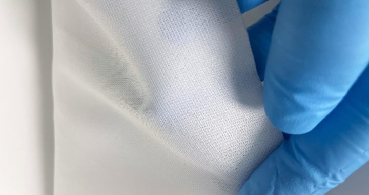
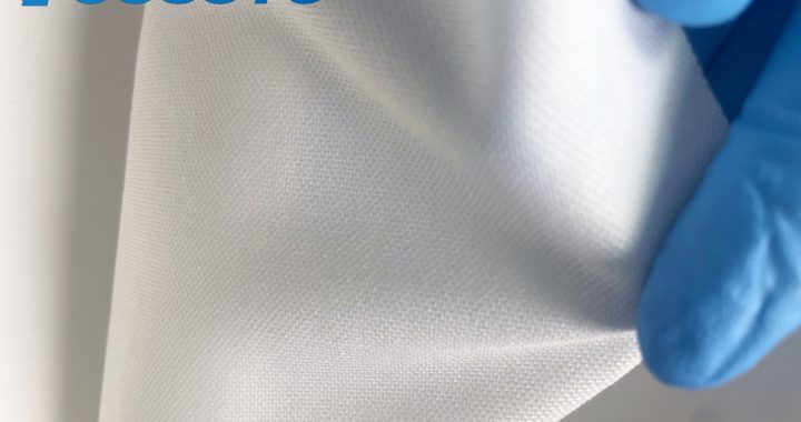
  • High-Density Wipe Selection:
    1. For flux residue (post-soldering) or organic oils: Choose high-density wipes pre-wet with 99% electronic-grade IPA (low impurities ≤10 ppb) to dissolve residues without damaging solder masks or SMDs.
    2. For water-soluble residues (e.g., cleaning agents from PCB fabrication): Use deionized water-based high-density wipes to avoid chemical reactions with metal traces.
    3. For anti-static needs: Select anti-static high-density wipes (surface resistance: 10⁶–10¹⁰ Ω) to prevent static from attracting dust back to the PCB.
  • Compatibility Check:
    1. Test the wipe on an inconspicuous area of the PCB (e.g., the edge of the substrate, not near components) to check for solder mask discoloration or swelling—wait 5 minutes before proceeding.

2. Step 1: Targeted Residue Removal (Flux, Oils, or Debris)

Use high-density wipes to eliminate specific contaminants without damaging delicate components:
  • Flux Residue on Solder Joints:
    1. Tear a high-density wipe into a narrow strip (1–2cm wide) to focus on small areas (avoids over-wiping adjacent components).
    2. Hold the wipe strip lightly against the flux-covered solder joint—apply minimal pressure (<0.3 psi) to avoid dislodging SMDs or bending component leads.
    3. Wipe the joint in single, slow linear strokes (parallel to the PCB surface) to dissolve and lift flux. Use a fresh section of the wipe for each joint to prevent cross-contamination.
  • Handling Oils on PCB Traces:
    1. Fold a full high-density wipe into a 4-layer pad (creates a firm, absorbent surface) to cover larger trace areas.
    2. Wipe the traces in the direction of their length (not across) to avoid scratching the thin copper layer. For narrow traces (≤0.1mm), use the edge of the folded wipe for precision.
  • Debris in Component Gaps (e.g., Between QFP Pins):
    1. Wrap a small section of the high-density wipe around the tip of plastic-tipped tweezers (avoids metal scratching).
    2. Gently insert the tweezers into the gap between component pins—move slowly to capture debris without bending pins. Discard the wipe section after use to prevent re-depositing debris.

3. Step 2: Post-Clean Rinse (For Water-Soluble Residues)

If using water-based high-density wipes, a final dry wipe prevents moisture damage to components:
  1. Use a dry high-density wipe (lint-free, same material as the wet wipe) to blot excess moisture from the PCB surface. Focus on component leads, connector pins, and IC sockets—moisture in these areas can cause corrosion or short circuits.
  2. For SMDs with underfill (e.g., BGA chips), gently dab the area with the dry wipe to remove surface moisture—do not press hard (risk of cracking the underfill).

4. Step 3: Post-Clean Inspection & Drying

Ensure the PCB is clean, dry, and ready for reuse or testing:
  1. Inspect the PCB under a 10–20x magnifying glass to check for:
    • Remaining residue (flux spots, oil streaks).
    • Lint or fiber debris (high-density wipes should leave ≤0.5 fibers per use—remove any with the bulb blower).
    • Damage (scratched traces, bent pins, or dislodged components).
  2. Allow the PCB to air-dry fully (10–15 minutes) in a clean, low-humidity area—ensure no moisture remains before reconnecting power or installing it back into equipment.
  3. For long-term storage, place the cleaned PCB in an ESD-safe bag with a desiccant packet to prevent dust accumulation and moisture damage.

Critical Prohibitions to Avoid PCB Damage

  • Do NOT use high-density wipes with harsh solvents (e.g., acetone, ethanol) on PCBs—they dissolve solder masks and damage plastic component housings.
  • Do NOT scrub or apply heavy pressure—this can dislodge SMDs, scratch copper traces, or peel solder masks.
  • Do NOT reuse high-density wipes—used wipes trap residue and debris, leading to cross-contamination or scratches.
By following this method, high-density cleanroom wipes deliver safe, thorough PCB cleaning in laboratories—preserving component integrity, ensuring electrical conductivity, and extending the lifespan of test and prototype PCBs.

Advantages of high-density dust-free cloth in PCB cleaning process

Printed Circuit Boards (PCBs)—especially those with fine-pitch components (0.4mm or smaller) and delicate surface-mount devices (SMDs)—require precise cleaning to remove flux residues, solder balls, and dust. High-density cleanroom wipes (250–400 gsm) outperform standard wipes in PCB workflows, offering unique benefits that protect component integrity, ensure electrical conductivity, and reduce rework. Below are their key advantages tailored to PCB cleaning tasks.

1. Superior Residue Removal: Eliminating Flux, Oil, and Solder Byproducts

Post-soldering flux residues (rosin-based or no-clean) and handling oils are major threats to PCB performance—they cause poor solder joint adhesion, corrosion, or electrical shorts. High-density wipes excel at residue removal due to:
  • Enhanced Solvent Retention: Their thick, porous fiber structure holds 12–15x their weight in solvents (e.g., 99% IPA, flux cleaners), allowing prolonged contact with stubborn residues. A single 300 gsm high-density wipe can dissolve and lift flux from 10+ SMD pads in one pass, vs. 2–3 standard wipes that dry out mid-task.
  • Targeted Cleaning Precision: The dense weave maintains shape when folded into narrow strips (1cm wide), enabling access to tight gaps between fine-pitch IC pins (e.g., QFP or BGA components). This prevents residue buildup in hard-to-reach areas that standard wipes miss—critical for avoiding “cold joints” or signal interference.
  • Uniform Solvent Release: Unlike standard wipes that drip or release solvent unevenly, high-density wipes distribute solvent consistently. This avoids streaks on PCB surfaces and prevents excess solvent from seeping into component housings (e.g., capacitors or IC chips), which can cause internal damage.

2. Low Linting & Particle Trapping: Protecting Fine-Pitch Components

Even tiny fiber debris or dust particles can short-circuit fine-pitch PCB traces (0.1mm or smaller) or block SMD contact points. High-density wipes mitigate this risk through:
  • Continuous-Filament Fibers: Made from lint-free polyester or microfiber (0.1μm diameter), they shed ≤0.5 fibers per use—far below the 2–5 fibers shed by standard staple-fiber wipes. This eliminates fiber contamination, a top cause of PCB test failures (e.g., “open circuit” errors due to fiber-blocked pads).
  • Micro-Particle Capture: Their tight weave traps particles as small as 0.05μm (e.g., solder balls, dust from handling). Testing shows high-density wipes remove 99.7% of sub-micron particles from PCB surfaces, vs. 85% for standard wipes—reducing rework rates by 30% in high-volume PCB assembly.

3. Durability & Reusability: Reducing Waste and Costs

PCB cleaning (especially batch processing) demands wipes that withstand repeated use without tearing—high-density wipes deliver long-lasting performance:
  • Tear & Fray Resistance: Reinforced fibers (e.g., high-tenacity polyester) and heat-sealed edges resist damage even when wiping rough solder masks or scraping gentle solder balls. They withstand 500+ folding cycles and 100+ wiping strokes on PCBs, vs. 100–200 cycles for standard wipes.
  • Reusable for Non-Critical Tasks: For pre-soldering dusting or post-cleaning surface checks, high-density wipes can be reused 3–5 times (when cleaned with mild detergent and air-dried). This cuts PCB cleaning supply costs by 40% vs. single-use standard wipes.

4. ESD Safety: Protecting ESD-Sensitive Components

Modern PCBs often include ESD-sensitive devices (e.g., microchips, sensors) that can be damaged by static discharge. High-density wipes offer reliable ESD protection:
  • Stable Anti-Static Performance: Anti-static high-density wipes (surface resistance: 10⁶–10¹⁰ Ω) maintain consistent charge dissipation even after solvent exposure or repeated use. They neutralize static in <0.1 seconds, preventing dust attraction to PCB traces and ESD-induced component failure.
  • Conductive Variants for High-Risk Tasks: For PCB assembly with ultra-sensitive components (e.g., RF chips), conductive high-density wipes (10³–10⁶ Ω) provide immediate charge grounding—eliminating the risk of static sparks that could damage delicate circuitry.

5. Compatibility with PCB Materials: No Surface Damage

PCBs feature diverse materials (FR-4 laminates, solder masks, gold-plated pads) that can be scratched or degraded by harsh wipes. High-density wipes are material-safe:
  • Soft Fiber Construction: Their plush, non-abrasive fibers avoid scratching solder masks or wearing down gold-plated contact pads—critical for PCBs used in aerospace or medical devices, where pad integrity impacts reliability.
  • Solvent Compatibility: They resist breakdown when used with PCB-specific solvents (e.g., flux removers, IPA), unlike standard wipes that disintegrate and leave fiber residue on PCBs.
By leveraging these advantages, high-density cleanroom wipes streamline PCB cleaning workflows, reduce defects, and lower long-term costs—making them indispensable for high-quality PCB manufacturing, repair, and maintenance.

Superior PCB Cleaning: Advantages of High-Density Wipes

Printed Circuit Boards (PCBs) in laboratory settings—used for sensor arrays, testing equipment, or prototype electronics—require meticulous cleaning to remove flux residues, solder debris, and dust. Even minor contamination can cause signal interference, short circuits, or component failure. High-density cleanroom wipes, with their thick, tightly woven structures and ultra-low linting properties, outperform standard wipes in PCB cleaning. Below are their key advantages, tailored to the unique demands of lab-based PCB maintenance and testing.

1. Superior Particle and Residue Trapping: Eliminates Microscopic Contaminants

Lab PCBs often feature fine-pitch components (0.4mm or smaller) and sensitive traces, where sub-micron particles or leftover flux can disrupt functionality. High-density wipes excel here by:
  • Dense Capillary Networks: Their tight weave (250–400 gsm) creates millions of tiny channels that trap particles as small as 0.05μm—far smaller than the 0.5μm particles standard wipes miss. This is critical for cleaning around SMDs (Surface-Mount Devices) or BGA (Ball Grid Array) packages, where dust can lodge between pins and cause connectivity issues.
  • Effective Flux Dissolution: When paired with high-purity solvents (e.g., 99% IPA), the thick, absorbent fibers of high-density wipes hold solvent longer, allowing it to fully dissolve rosin or no-clean flux residues. Unlike thin wipes that dry out quickly, high-density variants require fewer passes to remove stubborn flux—reducing the risk of scrubbing that can damage PCB traces.
  • Ultra-Low Linting: Made from continuous-filament polyester or microfiber, these wipes shed ≤1 fiber per use. This eliminates fiber contamination, a major cause of short circuits in lab PCBs (where even a single 1μm fiber can bridge adjacent traces).

2. Durability for Precision Handling: Avoids In-Use Damage

Lab PCBs are often prototypes or low-volume units, making damage during cleaning costly. High-density wipes protect PCBs by:
  • Tear and Fray Resistance: Reinforced, heat-sealed edges prevent fraying, even when wiping around sharp component leads or PCB edges. Standard wipes often tear during this process, leaving loose fibers or fragmented wipe material on the board.
  • Abrasion Protection: Their soft, plush texture glides over PCB surfaces without scratching solder masks or delicate component coatings (e.g., gold-plated pins). This is especially important for lab PCBs with exposed copper traces or optical sensors mounted directly on the board.
  • Reusable (When Approved): For non-critical lab PCBs (e.g., test fixtures), high-density wipes can be rinsed with solvent and reused, reducing waste. Their durable structure maintains performance through 3–5 uses, unlike standard wipes that degrade after a single pass.

3. Controlled Liquid Absorption: Prevents Solvent Damage

Over-saturating PCBs with solvent can seep into components (e.g., capacitors, ICs) and cause internal damage. High-density wipes address this by:
  • Uniform Solvent Retention: They absorb 10–15x their weight in solvent (e.g., IPA) and release it evenly, preventing drips or pooling on the PCB. This ensures consistent cleaning without risking solvent intrusion into component housings.
  • Fast, Streak-Free Drying: The dense fibers distribute solvent across the PCB surface, promoting rapid, even evaporation. This eliminates solvent streaks or residues that can attract dust later, reducing the need for re-cleaning.
  • Compatibility with Specialty Solvents: High-density wipes resist degradation from harsh PCB cleaning solvents (e.g., flux removers, acetone) that would break down standard wipes. This allows labs to use the most effective solvent for the job without compromising wipe performance.

4. Consistency for Lab Quality Control

Laboratory work demands repeatable results, and cleaning consistency is critical for reliable PCB testing. High-density wipes deliver this by:
  • Uniform Performance: Each wipe has the same thickness, fiber density, and absorption capacity, ensuring every PCB receives the same level of cleaning. This eliminates variability from standard wipes, which can have inconsistent fiber distribution.
  • Compliance with Lab Standards: Many high-density wipes meet ISO 14644-1 Class 5 standards and IPC-A-610 (electronics assembly guidelines), aligning with lab quality control requirements. This is essential for labs conducting regulated testing (e.g., aerospace or medical PCB validation).
For laboratories relying on PCBs for accurate testing or prototyping, high-density cleanroom wipes are a strategic choice—they protect delicate components, eliminate microscopic contamination, and ensure consistent cleaning results that support reliable lab work.