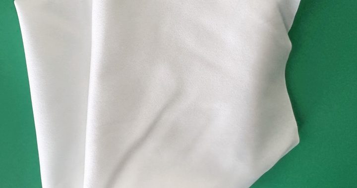
Printed Circuit Boards (PCBs)—used in electronics, sensors, and lab equipment—are highly vulnerable to electrostatic discharge (ESD) and particle contamination. Even tiny dust particles or static sparks can damage fine-pitch components (0.4mm or smaller) or cause short circuits. Anti-static cleanroom wipes are designed to mitigate these risks, but their effectiveness depends on proper application. Below are targeted tips to maximize cleaning results, protect PCB integrity, and maintain ESD safety during PCB cleaning workflows.
1. Pre-Cleaning Preparation: Set Up for ESD Safety & Contamination Control
Before touching the PCB, lay the groundwork to avoid introducing damage or debris:
- Ground Yourself and Workspace:
- Wear an ESD wrist strap (connected to a grounded workbench) and anti-static shoes to dissipate personal static charge (target: <100V).
- Place the PCB on an ESD-safe mat (surface resistance: 10⁶–10¹¹ Ω) to prevent charge buildup on the board itself.
- Select the Right Anti-Static Wipe:
- For dry dust removal (e.g., loose debris on PCB surfaces): Choose lint-free, static-dissipative microfiber wipes (200–250 gsm) with surface resistance 10⁶–10¹⁰ Ω. Avoid cotton or low-quality synthetic wipes—they shed fibers and generate static.
- For flux/residue removal (e.g., post-soldering): Use pre-moistened anti-static wipes with 99% high-purity IPA (safe for most PCB substrates and components). Ensure wipes are labeled “PCB-compatible” to avoid damaging solder masks or gold-plated pins.
- Inspect the PCB and Wipe:
- Check the PCB for loose components (e.g., SMDs, connectors) and secure them before cleaning—wipes can dislodge unstable parts.
- Verify the wipe is free of visible defects (e.g., frayed edges, stains) that could scratch the PCB or leave residues.
2. Dry Dust Removal: Gentle Techniques to Avoid Particle Spread
Dry cleaning is critical to remove loose dust before using solvents—rubbing dry particles into the PCB can scratch traces or lodge debris between components:
- Fold the Wipe for Precision:
- Fold the anti-static wipe into a 4-layer pad. This creates a smooth, dense cleaning surface (reduces fiber shedding) and provides multiple usable layers (rotate to a fresh layer when one becomes soiled).
- Use Light, Directional Strokes:
- Wipe along the PCB’s trace direction (not across) to avoid catching fibers on component leads. Apply pressure <1 psi—excessive force can bend delicate pins or damage solder joints.
- For tight spaces (e.g., between BGA packages or IC chips): Tear a small strip from the wipe and use tweezers to guide it—this prevents the wipe from snagging on components and spreading dust.
- Focus on High-Risk Areas:
- Pay extra attention to connector pins, solder joints, and IC leads—these areas trap dust that can cause connectivity issues. Use the edge of the folded wipe to reach into narrow gaps.
3. Solvent-Based Cleaning (Flux/Residue Removal): Control Moisture & ESD
When using pre-moistened anti-static wipes to remove flux, oil, or adhesive residues, avoid over-saturating the PCB or generating static:
- Limit Solvent Exposure:
- Do not soak the PCB—press the pre-moistened wipe lightly against the residue (hold for 5–10 seconds to let IPA dissolve it) before wiping. Over-saturating can seep into component housings (e.g., capacitors, ICs) and cause internal damage.
- For large flux deposits (e.g., around through-hole components), use a small amount of additional IPA on the wipe—avoid pouring IPA directly onto the PCB.
- Maintain ESD Control During Solvent Use:
- Ensure the pre-moistened wipe’s anti-static properties are intact (check the manufacturer’s label for solvent compatibility)—some wipes lose static-dissipative capabilities when exposed to harsh chemicals.
- Wipe in short, controlled strokes to minimize friction (friction generates static). If using a wipe for >1 minute, pause briefly to let any built-up charge dissipate through the ESD mat.
- Avoid Sensitive Components:
- Keep solvent-wetted wipes away from connectors, switches, and sensors—these parts are often not IP-rated and can fail if exposed to IPA. Use a dry anti-static wipe to clean these areas instead.
4. Post-Cleaning Inspection & Protection
After cleaning, verify results and protect the PCB from recontamination:
- Check for Residues and Damage:
- Inspect the PCB under a 10–20x magnifying glass for:
- IPA streaks (common on solder masks)—use a dry anti-static wipe to buff them away.
- Fiber debris (from low-quality wipes)—remove with a gentle blast of compressed air (static-neutralized).
- Component damage (e.g., bent pins, lifted traces)—address before proceeding with assembly or testing.
- Inspect the PCB under a 10–20x magnifying glass for:
- Store the Cleaned PCB Properly:
- Place the PCB in an anti-static bag or container immediately after cleaning. Avoid touching the cleaned surface with bare hands—skin oils reintroduce contaminants and static.
- Dispose of Wipes Safely:
- Discard used pre-moistened wipes in a fire-resistant bin (IPA is flammable). Dispose of dry wipes in standard ESD-safe waste—do not reuse them (they trap dust and will recontaminate PCBs).
By following these tips, anti-static cleanroom wipes effectively remove contaminants while protecting PCBs from ESD damage. This ensures reliable PCB performance, reduces rework costs, and maintains compliance with electronics assembly standards (e.g., IPC-A-610).
