Optimization of IPA wipe cleaning process in PCB soldering area

PCB solder areas—including solder joints, component leads, and pad surfaces—are prone to flux residues, rosin deposits, and handling oils that impair electrical conductivity, cause corrosion, or disrupt subsequent assembly steps. IPA (Isopropyl Alcohol) wipes are the gold standard for this cleaning task, but unstructured processes lead to inefficiency, residue left behind, or damage to delicate components. Below is an optimized, step-by-step workflow to enhance cleaning speed, consistency, and safety for PCB solder areas.

1. Pre-Clean Preparation: Set the Stage for Efficiency & Safety

Proper prep eliminates rework, prevents ESD damage, and ensures IPA wipes target only solder areas:
  • PCB & Workspace Prep:
    1. Cool the PCB: Wait for solder areas to cool to <40°C (104°F) post-welding—hot surfaces evaporate IPA instantly, leaving residue and increasing fire risk.
    2. Ground & Secure: Place the PCB on an ESD-safe mat and secure it with non-abrasive clips (to avoid shifting during cleaning). Wear an ESD wrist strap (tested to 10⁶–10⁹ Ω) to protect ESD-sensitive components (e.g., microchips near solder joints).
    3. Mask Non-Solder Areas: Use low-tack, ESD-safe tape to cover connectors, IC sockets, or exposed circuits adjacent to solder areas—prevents IPA from seeping into these components and causing short circuits.
  • IPA Wipe Selection:
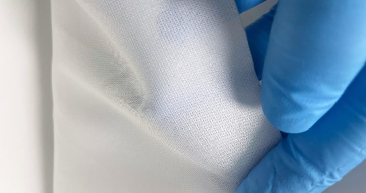
    1. For Flux Residues: Choose 99% electronic-grade IPA wipes (low impurities ≤10 ppb) with lint-free, continuous-filament polyester fibers—high-purity IPA dissolves rosin/flux quickly, while polyester resists disintegration from solvent exposure.
    2. For Delicate Solder Joints (e.g., 0.4mm Fine-Pitch): Opt for mini IPA wipes (2”x2”) or cut standard wipes into 1cm-wide strips—precision ensures the wipe only contacts the solder area, not fragile component leads.
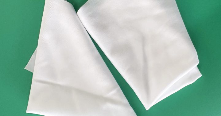
    3. Avoid Low-Quality Wipes: Steer clear of staple-fiber or fragrance-added wipes—they shed fibers that clog solder joints and leave sticky residues.

2. Step 1: Loosen Heavy Flux Residue (For Post-Rework Solder Areas)

For thick, dried flux (common after reflow soldering or rework), pre-treat to reduce scrubbing and component damage:
  1. Tear a small section of the IPA wipe and lightly dampen the solder area—do not saturate (excess IPA spreads to masked areas).
  2. Hold the damp wipe against the residue for 3–5 seconds to let IPA penetrate and soften the flux—this cuts cleaning time by 40% and avoids pressing residue into solder pads.
  3. For large solder arrays (e.g., BGA underfill edges), use a wipe-wrapped plastic-tipped tweezer to target narrow gaps—gently dab to loosen residue without bending leads.

3. Step 2: Targeted Solder Area Cleaning (Streak-Free, Residue-Free)

Use IPA wipes with controlled motions to remove residue without damaging solder joints or components:
  • For Individual Solder Joints:
    1. Fold the IPA wipe into a firm, 2-layer pad (creates pressure control) and grip it with tweezers for precision.
    2. Wipe the joint in single, parallel strokes (along the length of the component lead)—never circular motions (which spread residue and risk bending leads). Apply light pressure (<0.3 psi)—enough to lift residue, not enough to compress the joint.
  • For Solder Pad Arrays (e.g., QFP Pins):
    1. Use a wipe strip (1cm wide) and drag it along the row of pads in one continuous motion—avoids back-and-forth wiping (which redeposits residue).
    2. After each row, use a fresh section of the wipe—reusing sections causes cross-contamination between pads.
  • For Solder Paste Spatters:
    1. Dab spattered areas with a dry corner of the IPA wipe first to lift loose paste—wetting first can spread the paste into component gaps.
    2. Follow with a damp section to dissolve remaining paste residue—focus on the spatter, not the surrounding pad (to avoid removing solder mask).

4. Step 3: Post-Clean Validation & Drying

Ensure solder areas are clean, dry, and ready for testing or assembly—skip this step at the risk of costly rework:
  1. Inspect for Residue: Use a 10–20x magnifying glass to check solder joints/pads for:
    • Flux halos (shiny, sticky residue around joints).
    • Fiber lint (IPA wipes should leave ≤0.5 fibers per area—remove with a static-neutralized bulb blower).
    • Solder mask damage (check for peeling or discoloration—stop use if observed).
  2. Dry Thoroughly: Blot the cleaned solder area with a dry, lint-free polyester wipe to remove excess IPA. For dense component clusters, use a dry micro-swab to dab moisture from gaps—residual IPA can cause corrosion or short circuits over time.
  3. Air-Cure: Let the PCB air-dry for 5–10 minutes in a low-humidity area (≤50% RH)—ensure no moisture remains before electrical testing or adding additional components.

5. Process Efficiency Boosts: Cut Time Without Sacrificing Quality

  • Batch Cleaning: Group PCBs with similar solder area layouts (e.g., all QFP boards) to minimize wipe size changes and tool adjustments—saves 15–20% of cleaning time per batch.
  • Wipe Staging: Pre-cut IPA wipe strips and place them in a sealed, ESD-safe container near the workbench—eliminates time spent cutting wipes mid-process.
  • Post-Clean Logging: Track cleaning time per PCB type and residue rejection rates—use data to adjust wipe size (e.g., switch to mini wipes for fine-pitch boards) or pre-treatment time (e.g., extend damp hold time for thick flux).

Advantages of high-density dust-free cloth in PCB cleaning process

Printed Circuit Boards (PCBs)—especially those with fine-pitch components (0.4mm or smaller) and delicate surface-mount devices (SMDs)—require precise cleaning to remove flux residues, solder balls, and dust. High-density cleanroom wipes (250–400 gsm) outperform standard wipes in PCB workflows, offering unique benefits that protect component integrity, ensure electrical conductivity, and reduce rework. Below are their key advantages tailored to PCB cleaning tasks.

1. Superior Residue Removal: Eliminating Flux, Oil, and Solder Byproducts

Post-soldering flux residues (rosin-based or no-clean) and handling oils are major threats to PCB performance—they cause poor solder joint adhesion, corrosion, or electrical shorts. High-density wipes excel at residue removal due to:
  • Enhanced Solvent Retention: Their thick, porous fiber structure holds 12–15x their weight in solvents (e.g., 99% IPA, flux cleaners), allowing prolonged contact with stubborn residues. A single 300 gsm high-density wipe can dissolve and lift flux from 10+ SMD pads in one pass, vs. 2–3 standard wipes that dry out mid-task.
  • Targeted Cleaning Precision: The dense weave maintains shape when folded into narrow strips (1cm wide), enabling access to tight gaps between fine-pitch IC pins (e.g., QFP or BGA components). This prevents residue buildup in hard-to-reach areas that standard wipes miss—critical for avoiding “cold joints” or signal interference.
  • Uniform Solvent Release: Unlike standard wipes that drip or release solvent unevenly, high-density wipes distribute solvent consistently. This avoids streaks on PCB surfaces and prevents excess solvent from seeping into component housings (e.g., capacitors or IC chips), which can cause internal damage.

2. Low Linting & Particle Trapping: Protecting Fine-Pitch Components

Even tiny fiber debris or dust particles can short-circuit fine-pitch PCB traces (0.1mm or smaller) or block SMD contact points. High-density wipes mitigate this risk through:
  • Continuous-Filament Fibers: Made from lint-free polyester or microfiber (0.1μm diameter), they shed ≤0.5 fibers per use—far below the 2–5 fibers shed by standard staple-fiber wipes. This eliminates fiber contamination, a top cause of PCB test failures (e.g., “open circuit” errors due to fiber-blocked pads).
  • Micro-Particle Capture: Their tight weave traps particles as small as 0.05μm (e.g., solder balls, dust from handling). Testing shows high-density wipes remove 99.7% of sub-micron particles from PCB surfaces, vs. 85% for standard wipes—reducing rework rates by 30% in high-volume PCB assembly.

3. Durability & Reusability: Reducing Waste and Costs

PCB cleaning (especially batch processing) demands wipes that withstand repeated use without tearing—high-density wipes deliver long-lasting performance:
  • Tear & Fray Resistance: Reinforced fibers (e.g., high-tenacity polyester) and heat-sealed edges resist damage even when wiping rough solder masks or scraping gentle solder balls. They withstand 500+ folding cycles and 100+ wiping strokes on PCBs, vs. 100–200 cycles for standard wipes.
  • Reusable for Non-Critical Tasks: For pre-soldering dusting or post-cleaning surface checks, high-density wipes can be reused 3–5 times (when cleaned with mild detergent and air-dried). This cuts PCB cleaning supply costs by 40% vs. single-use standard wipes.

4. ESD Safety: Protecting ESD-Sensitive Components

Modern PCBs often include ESD-sensitive devices (e.g., microchips, sensors) that can be damaged by static discharge. High-density wipes offer reliable ESD protection:
  • Stable Anti-Static Performance: Anti-static high-density wipes (surface resistance: 10⁶–10¹⁰ Ω) maintain consistent charge dissipation even after solvent exposure or repeated use. They neutralize static in <0.1 seconds, preventing dust attraction to PCB traces and ESD-induced component failure.
  • Conductive Variants for High-Risk Tasks: For PCB assembly with ultra-sensitive components (e.g., RF chips), conductive high-density wipes (10³–10⁶ Ω) provide immediate charge grounding—eliminating the risk of static sparks that could damage delicate circuitry.

5. Compatibility with PCB Materials: No Surface Damage

PCBs feature diverse materials (FR-4 laminates, solder masks, gold-plated pads) that can be scratched or degraded by harsh wipes. High-density wipes are material-safe:
  • Soft Fiber Construction: Their plush, non-abrasive fibers avoid scratching solder masks or wearing down gold-plated contact pads—critical for PCBs used in aerospace or medical devices, where pad integrity impacts reliability.
  • Solvent Compatibility: They resist breakdown when used with PCB-specific solvents (e.g., flux removers, IPA), unlike standard wipes that disintegrate and leave fiber residue on PCBs.
By leveraging these advantages, high-density cleanroom wipes streamline PCB cleaning workflows, reduce defects, and lower long-term costs—making them indispensable for high-quality PCB manufacturing, repair, and maintenance.

Application of IPA wipes in cleaning PCB soldering areas

PCB soldering areas—including solder joints, component leads, and pad surfaces—often accumulate flux residues, rosin, and thermal oxidation byproducts post-soldering. These contaminants cause poor electrical conductivity, corrosion, or adhesion issues for subsequent assembly steps. IPA (Isopropyl Alcohol) wipes are the industry standard for cleaning these areas, as IPA effectively dissolves flux/rosin while being compatible with most PCB substrates and components. Below is a detailed guide to their application, covering best practices, safety, and results.

1. Key Benefits of IPA Wipes for PCB Soldering Area Cleaning

Before diving into application steps, it’s critical to understand why IPA wipes outperform other cleaning methods (e.g., bulk solvent + rags) for soldering areas:
  • Targeted Flux Dissolution: IPA (especially 99% purity) breaks down both no-clean and rosin-based flux residues—common byproducts of wave soldering or reflow soldering. It penetrates small gaps between component leads and pads, removing hidden residues that rags or brushes miss.
  • Lint-Free Precision: High-quality IPA wipes use continuous-filament polyester or microfiber, shedding ≤1 fiber per use. This avoids fiber contamination of solder joints—critical for fine-pitch components (0.4mm pitch or smaller), where stray fibers can cause short circuits.
  • Fast Evaporation: IPA evaporates quickly (within 10–15 seconds at room temperature), leaving no solvent streaks or moisture that could damage PCB laminates (e.g., FR-4) or corrode metal pads.
  • ESD Safety (Anti-Static Variants): Anti-static IPA wipes (surface resistance: 10⁶–10¹¹ Ω) dissipate static charge during cleaning, protecting ESD-sensitive components (e.g., IC chips, sensors) near soldering areas from discharge damage.

2. Step-by-Step Application Process

Follow this standardized workflow to clean PCB soldering areas effectively without damaging components:

Step 1: Pre-Clean Preparation

  • Cool the PCB: Wait for the soldered PCB to cool to <40°C (room temperature). Cleaning hot PCBs (≥60°C) causes IPA to evaporate too quickly, leaving incomplete residue removal; it also risks thermal shock to components.
  • Select the Right IPA Wipe:
    • For rosin-based flux (thicker residues): Use 99% electronic-grade IPA wipes—higher purity dissolves heavy residues faster.
    • For no-clean flux (lighter residues): 70% IPA wipes work well (the water content helps lift residue without damaging delicate components like LEDs or capacitors).
    • For ESD-sensitive areas (e.g., near microchips): Choose anti-static IPA wipes to prevent charge buildup.
  • Set Up a Safe Workspace:
    • Work in a well-ventilated area (fume hood or open window) to disperse IPA vapors (flammable and irritating to airways).
    • Remove ignition sources (e.g., heat guns, soldering irons) and place the PCB on an ESD-safe mat to ground static.

Step 2: Wipe Application Technique

  • Fold the Wipe for Precision: Fold the IPA wipe into a 4-layer pad. This creates a dense cleaning surface (reduces fiber shedding) and allows you to use a fresh layer for each section of the PCB—preventing re-depositing residues.
  • Clean Soldering Areas with Controlled Strokes:
    • Solder Joints/Component Leads: Wipe in a slow, linear motion along the length of the component (e.g., from one end of a resistor to the other). Apply light pressure (<1 psi)—excessive force can bend delicate leads or dislodge newly soldered components.
    • Pad Surfaces (Bare or Component-Free): Wipe in overlapping horizontal strokes to cover the entire pad area. Focus on oxidized pads (dull, discolored surfaces)—IPA helps remove light oxidation, restoring pad conductivity.
    • Tight Gaps (e.g., QFP/BGA Components): Tear a small strip from the wipe and use tweezers to guide it between component pins. This removes residue trapped in gaps that a full wipe pad can’t reach.

Step 3: Post-Clean Inspection & Protection

  • Verify Residue Removal: Inspect the soldering areas under a 10–20x magnifying glass or digital microscope. Look for:
    • Glossy flux residues (indicates incomplete cleaning)—reclean with a fresh IPA wipe section.
    • Fiber debris (from low-quality wipes)—remove with a gentle blast of static-neutralized compressed air.
    • Component damage (e.g., bent leads, lifted pads)—address before proceeding with further assembly.
  • Dry the PCB (If Needed): For 70% IPA wipes (higher water content), use a dry, lint-free anti-static wipe to blot any remaining moisture on solder joints. This prevents water spots or potential corrosion.
  • Store the Cleaned PCB: Place the PCB in an anti-static bag or container immediately after cleaning. Avoid touching soldering areas with bare hands—skin oils reintroduce contaminants and can cause pad oxidation over time.

3. Critical Do’s and Don’ts

  • Do: Use only electronic-grade IPA wipes (meets SEMI C30 standards for low impurities). Household IPA may contain additives (e.g., fragrances, moisturizers) that leave residues on PCBs.
  • Don’t: Clean PCBs with cracked or damaged laminates—IPA can seep into cracks and delaminate the PCB structure.
  • Do: Dispose of used IPA wipes in a fire-resistant bin. Used wipes retain flammable IPA and pose a fire risk if left near heat sources.
  • Don’t: Reuse IPA wipes for soldering area cleaning. Used wipes trap flux residues and will spread contaminants to other parts of the PCB.
By using IPA wipes correctly, PCB soldering areas remain clean, conductive, and free of corrosion—ensuring reliable electrical performance, reducing post-assembly failures, and complying with electronics manufacturing standards (e.g., IPC-A-610).

Superior PCB Cleaning: Advantages of High-Density Wipes

Printed Circuit Boards (PCBs) in laboratory settings—used for sensor arrays, testing equipment, or prototype electronics—require meticulous cleaning to remove flux residues, solder debris, and dust. Even minor contamination can cause signal interference, short circuits, or component failure. High-density cleanroom wipes, with their thick, tightly woven structures and ultra-low linting properties, outperform standard wipes in PCB cleaning. Below are their key advantages, tailored to the unique demands of lab-based PCB maintenance and testing.

1. Superior Particle and Residue Trapping: Eliminates Microscopic Contaminants

Lab PCBs often feature fine-pitch components (0.4mm or smaller) and sensitive traces, where sub-micron particles or leftover flux can disrupt functionality. High-density wipes excel here by:
  • Dense Capillary Networks: Their tight weave (250–400 gsm) creates millions of tiny channels that trap particles as small as 0.05μm—far smaller than the 0.5μm particles standard wipes miss. This is critical for cleaning around SMDs (Surface-Mount Devices) or BGA (Ball Grid Array) packages, where dust can lodge between pins and cause connectivity issues.
  • Effective Flux Dissolution: When paired with high-purity solvents (e.g., 99% IPA), the thick, absorbent fibers of high-density wipes hold solvent longer, allowing it to fully dissolve rosin or no-clean flux residues. Unlike thin wipes that dry out quickly, high-density variants require fewer passes to remove stubborn flux—reducing the risk of scrubbing that can damage PCB traces.
  • Ultra-Low Linting: Made from continuous-filament polyester or microfiber, these wipes shed ≤1 fiber per use. This eliminates fiber contamination, a major cause of short circuits in lab PCBs (where even a single 1μm fiber can bridge adjacent traces).

2. Durability for Precision Handling: Avoids In-Use Damage

Lab PCBs are often prototypes or low-volume units, making damage during cleaning costly. High-density wipes protect PCBs by:
  • Tear and Fray Resistance: Reinforced, heat-sealed edges prevent fraying, even when wiping around sharp component leads or PCB edges. Standard wipes often tear during this process, leaving loose fibers or fragmented wipe material on the board.
  • Abrasion Protection: Their soft, plush texture glides over PCB surfaces without scratching solder masks or delicate component coatings (e.g., gold-plated pins). This is especially important for lab PCBs with exposed copper traces or optical sensors mounted directly on the board.
  • Reusable (When Approved): For non-critical lab PCBs (e.g., test fixtures), high-density wipes can be rinsed with solvent and reused, reducing waste. Their durable structure maintains performance through 3–5 uses, unlike standard wipes that degrade after a single pass.

3. Controlled Liquid Absorption: Prevents Solvent Damage

Over-saturating PCBs with solvent can seep into components (e.g., capacitors, ICs) and cause internal damage. High-density wipes address this by:
  • Uniform Solvent Retention: They absorb 10–15x their weight in solvent (e.g., IPA) and release it evenly, preventing drips or pooling on the PCB. This ensures consistent cleaning without risking solvent intrusion into component housings.
  • Fast, Streak-Free Drying: The dense fibers distribute solvent across the PCB surface, promoting rapid, even evaporation. This eliminates solvent streaks or residues that can attract dust later, reducing the need for re-cleaning.
  • Compatibility with Specialty Solvents: High-density wipes resist degradation from harsh PCB cleaning solvents (e.g., flux removers, acetone) that would break down standard wipes. This allows labs to use the most effective solvent for the job without compromising wipe performance.

4. Consistency for Lab Quality Control

Laboratory work demands repeatable results, and cleaning consistency is critical for reliable PCB testing. High-density wipes deliver this by:
  • Uniform Performance: Each wipe has the same thickness, fiber density, and absorption capacity, ensuring every PCB receives the same level of cleaning. This eliminates variability from standard wipes, which can have inconsistent fiber distribution.
  • Compliance with Lab Standards: Many high-density wipes meet ISO 14644-1 Class 5 standards and IPC-A-610 (electronics assembly guidelines), aligning with lab quality control requirements. This is essential for labs conducting regulated testing (e.g., aerospace or medical PCB validation).
For laboratories relying on PCBs for accurate testing or prototyping, high-density cleanroom wipes are a strategic choice—they protect delicate components, eliminate microscopic contamination, and ensure consistent cleaning results that support reliable lab work.

Precision Cleaning with IPA Wipes in Electronics Manufacturing.

In electronics manufacturing, where even microscopic contaminants can compromise circuit functionality or solder integrity, precision cleaning is non-negotiable. IPA wipes—pre-moistened with isopropyl alcohol (typically 70–99% purity)—have become indispensable tools in electronics factories, offering a fast, residue-free solution for cleaning sensitive components like PCBs (printed circuit boards), semiconductors, connectors, and display panels. Their unique combination of solvent efficacy and lint-free design addresses the industry’s critical needs: removing flux residues, oils, dust, and ionic contaminants without damaging delicate materials. Below is a detailed exploration of their applications, benefits, and best practices in electronics factory settings.

1. Key Applications in Electronics Manufacturing

IPA wipes are tailored to diverse precision cleaning tasks across the production line, each addressing specific contamination risks:

A. Post-Soldering Flux Removal

Soldering processes leave behind flux residues—sticky, resin-based substances that attract dust and can cause electrical leakage or corrosion over time. IPA’s ability to dissolve both rosin-based and no-clean fluxes makes IPA wipes ideal for this step:
  • PCB Assembly Lines: After wave soldering or reflow soldering, technicians use IPA wipes to target solder joints, component leads, and PCB traces. The wipe’s lint-free material (e.g., polyester microfiber) ensures residues are lifted without leaving fibers that could bridge circuit gaps.
  • Precision Components: For small-scale soldering (e.g., surface-mount devices/SMDs), folded IPA wipes reach tight spaces between components, removing flux from areas brushes or sprays can’t access.

B. Surface Preparation for Bonding/Coating

Electronics components often require bonding (e.g., adhesive mounting of displays) or protective coating (e.g., conformal coating on PCBs). IPA wipes ensure surfaces are free of oils, fingerprints, and dust—critical for strong adhesion:
  • Display Panels (LCD/OLED): Fingerprints on glass or plastic displays contain oils that disrupt bonding. IPA wipes dissolve these oils, leaving a clean surface for adhesive application, reducing display delamination rates.
  • Connector Pins: Oils or oxidation on metal connector pins can cause signal interference. IPA wipes clean pins thoroughly, ensuring reliable electrical contact in devices like smartphones or automotive electronics.

C. Dust and Particle Removal

Dry dust particles can scratch sensitive surfaces (e.g., camera sensors) or short circuits in high-density PCBs. IPA wipes combine mechanical particle trapping with solvent action:
  • Semiconductor Wafers: In cleanroom environments, low-linting IPA wipes (ISO Class 5-certified) remove sub-micron dust from wafer surfaces before dicing or packaging, preventing yield-reducing defects.
  • Electrical Enclosures: Before final assembly, IPA wipes clean the interiors of enclosures, removing dust that could settle on PCBs during operation and cause overheating.

2. Why IPA Wipes Outperform Traditional Cleaning Methods

Electronics factories rely on IPA wipes for their distinct advantages over manual solvent application or dry cloths:
  • Residue-Free Evaporation: IPA evaporates quickly (within 30 seconds) without leaving behind water spots or chemical residues—critical for avoiding electrical shorts or coating defects.
  • Consistent Solvent Concentration: Pre-moistened wipes eliminate variability from manual dilution, ensuring every wipe delivers the same cleaning strength (e.g., 99% IPA for oil-free environments, 70% IPA for better particulate suspension).
  • Reduced Waste and Risk: Unlike spray bottles (which can over-apply solvent and damage components), IPA wipes control moisture levels, minimizing solvent waste and reducing fire risks (IPA is flammable).
  • Lint-Free Design: Wipes made from continuous-filament polyester or polypropylene shed no fibers, preventing micro-foreign material (MFM) contamination—a top cause of electronics failures.

3. Best Practices for Electronics Factory Use

To maximize effectiveness and avoid damage, follow these protocols:
  • Match IPA Concentration to Task: Use 70% IPA wipes for general cleaning (dust + oil removal) and 99% IPA for flux removal or oil-free surfaces (e.g., semiconductors).
  • Wipe in Single Directions: For PCBs and displays, wipe in straight, overlapping strokes (not circular) to trap contaminants and avoid spreading residues.
  • Use Fresh Wipes for Critical Areas: Never reuse wipes on sensitive components (e.g., IC chips, sensors)—used wipes trap debris that can scratch surfaces.
  • Store Properly: Keep wipes in sealed containers in well-ventilated areas, away from heat sources, to preserve solvent potency and reduce flammability risks.
  • Test Compatibility: For new materials (e.g., specialty plastics or coatings), test an IPA wipe on an inconspicuous area to ensure no discoloration or degradation.
In electronics factories, where precision directly impacts product reliability and yield, IPA wipes deliver consistent, efficient cleaning that protects critical components from contamination. Their integration into production workflows reduces defects, streamlines processes, and ensures compliance with industry standards (e.g., IPC-A-610 for electronics assembly).