IPA Rag Alcohol Operation Guide for PCB Cleaning

PCBs (Printed Circuit Boards) require thorough, residue-free cleaning to eliminate flux, solder spatter, handling oils, and dust—contaminants that cause electrical shorts, poor solder joints, or component failure. IPA (Isopropyl Alcohol) wipes—pre-impregnated with 70–99% electronic-grade IPA—deliver safe, effective solvent-based cleaning for PCBs, from prototype repair to high-volume production. Below is a step-by-step operation guide to protect PCB integrity while ensuring deep decontamination.

1. Pre-Clean Preparation: Safety, Compatibility, and Tool Setup

Lay the groundwork to avoid PCB damage and ensure targeted cleaning:
  • Safety Precautions:
    1. Work in a well-ventilated area (IPA is volatile)—avoid enclosed spaces to prevent vapor buildup.
    2. Wear nitrile gloves (low-lint, chemical-resistant) to prevent skin oil transfer to PCBs and protect hands from IPA.
    3. Power off and disconnect any mounted components (e.g., microchips, resistors) from the PCB—IPA is conductive, so live circuits risk shorting.
  • IPA Wipe Selection:
    PCB Contaminant Type IPA Concentration Wipe Material Purpose
    Flux residue (rosin/no-clean) 99% electronic-grade Lint-free polyester Dissolves tough flux without residue
    Handling oils/fingerprints 70% electronic-grade Cellulose-polyester blend Balances solvent strength and surface safety
    Solder spatter/metal dust 99% electronic-grade High-density polyester Captures debris while dissolving oils
  • Tool Prep:

    Gather a static-neutralized bulb blower, 10–20x PCB magnifier, and dry lint-free cloth (for post-wipe drying). Secure the PCB on an anti-static mat to prevent ESD damage.

2. Step 1: Remove Loose Dust & Debris (Pre-IPA Pass)

Wiping loose particles with IPA wipes grinds them into PCB traces or component leads—always eliminate dry contaminants first:
  1. Use the static-neutralized bulb blower to deliver short, gentle bursts of air to the PCB surface. Focus on tight areas: component gaps, solder joints, and connector pins. Tilt the PCB at a 45° angle to let dust fall downward (not onto other components).
  2. For stubborn dust (e.g., trapped between 0201 resistors), use a dry, lint-free micro-swab (wooden handle—avoids ESD) to lightly dab the area. Discard the swab after use to prevent cross-contamination.
  3. Inspect the PCB under the magnifier—proceed to IPA cleaning only if no visible dust remains.

3. Step 2: IPA Wipe Cleaning (Targeted Contaminant Removal)

Follow these techniques to dissolve residues without damaging PCB materials (e.g., solder masks, copper traces):
  • General Surface Cleaning (Open PCB Areas):
    1. Remove one IPA wipe from its sealed packaging—hold it by the edges (never touch the cleaning surface) to avoid fiber transfer.
    2. Wipe the PCB in slow, linear strokes (parallel to copper traces)—never circular motions (which spread contaminants and risk scratching the solder mask). Apply light pressure (<0.2 psi)—enough to lift residue, not enough to bend delicate leads.
  • Precision Cleaning (Component Leads/Fine-Pitch Pads):
    1. For narrow areas (e.g., QFP/BGA pins, 0.3mm pitch connectors), tear the IPA wipe into 1cm-wide strips.
    2. Wrap a strip around the tip of plastic-tipped tweezers (avoids metal scratching) and gently run it along component leads or between pads. Rotate the tweezers to use a fresh section of the strip for each pass.
  • Flux Residue Removal:
    1. Hold the IPA wipe against dried flux spots (e.g., around solder joints) for 2–3 seconds—this softens the flux, reducing the need for scrubbing.
    2. Wipe the flux spot in a single, gentle stroke—repeating with a fresh wipe section if residue remains. Avoid over-wiping (can wear away the solder mask).

4. Step 3: Post-Clean Drying & Validation

Residual IPA causes water spots or flux re-deposition as it evaporates—proper drying ensures a clean finish:
  1. Blot Excess IPA: Immediately after cleaning, use a dry lint-free cloth to lightly blot the PCB surface. Use a single pass—rubbing smears remaining residue and risks damaging components.
  2. Air-Dry Fully: Let the PCB air-dry for 5–10 minutes in a low-humidity area (≤50% RH). For PCBs with fine-pitch components, extend drying time to 15 minutes—trapped IPA in small gaps can corrode traces over time.
  3. Validation:
  • Inspect the PCB under the 10–20x magnifier for remaining flux, fibers, or discoloration—no contaminants should be visible.
  • For functional PCBs, use a multimeter to check for continuity between traces (ensures no IPA-induced shorts) before remounting components.

5. Critical Do’s & Don’ts

  • Do: Test IPA wipes on an inconspicuous PCB area (e.g., edge of the solder mask) first—ensure no discoloration or mask peeling.
  • Don’t: Use IPA wipes on PCB materials like flexible polyimide (some grades are IPA-sensitive)—check the PCB manufacturer’s guidelines.
  • Do: Dispose of used IPA wipes in fire-resistant bins (IPA is flammable)—never discard in regular trash.
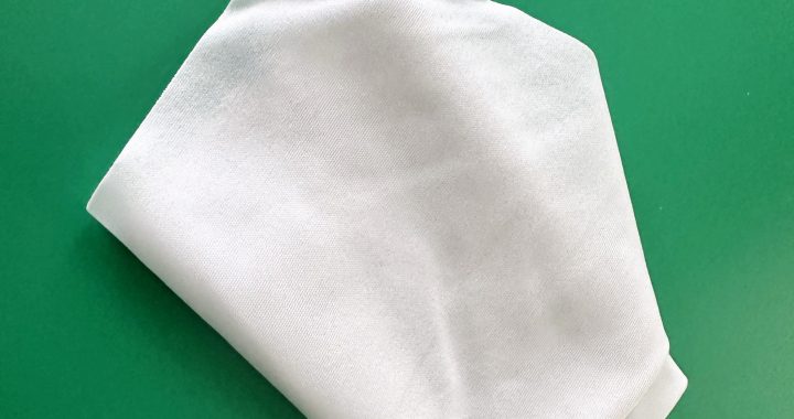
Optimization of IPA wipe cleaning process in PCB soldering area

PCB solder areas—including solder joints, component leads, and pad surfaces—are prone to flux residues, rosin deposits, and handling oils that impair electrical conductivity, cause corrosion, or disrupt subsequent assembly steps. IPA (Isopropyl Alcohol) wipes are the gold standard for this cleaning task, but unstructured processes lead to inefficiency, residue left behind, or damage to delicate components. Below is an optimized, step-by-step workflow to enhance cleaning speed, consistency, and safety for PCB solder areas.

1. Pre-Clean Preparation: Set the Stage for Efficiency & Safety

Proper prep eliminates rework, prevents ESD damage, and ensures IPA wipes target only solder areas:
  • PCB & Workspace Prep:
    1. Cool the PCB: Wait for solder areas to cool to <40°C (104°F) post-welding—hot surfaces evaporate IPA instantly, leaving residue and increasing fire risk.
    2. Ground & Secure: Place the PCB on an ESD-safe mat and secure it with non-abrasive clips (to avoid shifting during cleaning). Wear an ESD wrist strap (tested to 10⁶–10⁹ Ω) to protect ESD-sensitive components (e.g., microchips near solder joints).
    3. Mask Non-Solder Areas: Use low-tack, ESD-safe tape to cover connectors, IC sockets, or exposed circuits adjacent to solder areas—prevents IPA from seeping into these components and causing short circuits.
  • IPA Wipe Selection:
    1. For Flux Residues: Choose 99% electronic-grade IPA wipes (low impurities ≤10 ppb) with lint-free, continuous-filament polyester fibers—high-purity IPA dissolves rosin/flux quickly, while polyester resists disintegration from solvent exposure.
    2. For Delicate Solder Joints (e.g., 0.4mm Fine-Pitch): Opt for mini IPA wipes (2”x2”) or cut standard wipes into 1cm-wide strips—precision ensures the wipe only contacts the solder area, not fragile component leads.
    3. Avoid Low-Quality Wipes: Steer clear of staple-fiber or fragrance-added wipes—they shed fibers that clog solder joints and leave sticky residues.

2. Step 1: Loosen Heavy Flux Residue (For Post-Rework Solder Areas)

For thick, dried flux (common after reflow soldering or rework), pre-treat to reduce scrubbing and component damage:
  1. Tear a small section of the IPA wipe and lightly dampen the solder area—do not saturate (excess IPA spreads to masked areas).
  2. Hold the damp wipe against the residue for 3–5 seconds to let IPA penetrate and soften the flux—this cuts cleaning time by 40% and avoids pressing residue into solder pads.
  3. For large solder arrays (e.g., BGA underfill edges), use a wipe-wrapped plastic-tipped tweezer to target narrow gaps—gently dab to loosen residue without bending leads.

3. Step 2: Targeted Solder Area Cleaning (Streak-Free, Residue-Free)

Use IPA wipes with controlled motions to remove residue without damaging solder joints or components:
  • For Individual Solder Joints:
    1. Fold the IPA wipe into a firm, 2-layer pad (creates pressure control) and grip it with tweezers for precision.
    2. Wipe the joint in single, parallel strokes (along the length of the component lead)—never circular motions (which spread residue and risk bending leads). Apply light pressure (<0.3 psi)—enough to lift residue, not enough to compress the joint.
  • For Solder Pad Arrays (e.g., QFP Pins):
    1. Use a wipe strip (1cm wide) and drag it along the row of pads in one continuous motion—avoids back-and-forth wiping (which redeposits residue).
    2. After each row, use a fresh section of the wipe—reusing sections causes cross-contamination between pads.
  • For Solder Paste Spatters:
    1. Dab spattered areas with a dry corner of the IPA wipe first to lift loose paste—wetting first can spread the paste into component gaps.
    2. Follow with a damp section to dissolve remaining paste residue—focus on the spatter, not the surrounding pad (to avoid removing solder mask).

4. Step 3: Post-Clean Validation & Drying

Ensure solder areas are clean, dry, and ready for testing or assembly—skip this step at the risk of costly rework:
  1. Inspect for Residue: Use a 10–20x magnifying glass to check solder joints/pads for:
    • Flux halos (shiny, sticky residue around joints).
    • Fiber lint (IPA wipes should leave ≤0.5 fibers per area—remove with a static-neutralized bulb blower).
    • Solder mask damage (check for peeling or discoloration—stop use if observed).
  2. Dry Thoroughly: Blot the cleaned solder area with a dry, lint-free polyester wipe to remove excess IPA. For dense component clusters, use a dry micro-swab to dab moisture from gaps—residual IPA can cause corrosion or short circuits over time.
  3. Air-Cure: Let the PCB air-dry for 5–10 minutes in a low-humidity area (≤50% RH)—ensure no moisture remains before electrical testing or adding additional components.

5. Process Efficiency Boosts: Cut Time Without Sacrificing Quality

  • Batch Cleaning: Group PCBs with similar solder area layouts (e.g., all QFP boards) to minimize wipe size changes and tool adjustments—saves 15–20% of cleaning time per batch.
  • Wipe Staging: Pre-cut IPA wipe strips and place them in a sealed, ESD-safe container near the workbench—eliminates time spent cutting wipes mid-process.
  • Post-Clean Logging: Track cleaning time per PCB type and residue rejection rates—use data to adjust wipe size (e.g., switch to mini wipes for fine-pitch boards) or pre-treatment time (e.g., extend damp hold time for thick flux).