Anti-Static Wipes for Semiconductor Equipment Cleaning

Semiconductor equipment—including lithography tools, wafer chucks, and transfer robots—operates in ultra-sensitive ISO Class 1–5 cleanrooms, where even sub-micron particles or electrostatic discharge (ESD) can ruin 5nm/3nm wafers, damage delicate sensors, or halt production. Anti-static cleanroom wipes are purpose-built to address these risks, outperforming standard wipes by combining contamination control with static dissipation. Their unique design and material properties deliver critical advantages that safeguard semiconductor equipment integrity and ensure consistent manufacturing quality. Below is a detailed breakdown of their key benefits.

1. ESD Protection: Eliminates Costly Static-Related Damage

ESD is a top threat in semiconductor facilities: a single static discharge (as low as 50V) can damage ESD-sensitive components (ESDs) like wafer sensors, IC chips, or lithography optics. Anti-static cleanroom wipes mitigate this risk through:
  • Static-Dissipative Materials: Wipes are crafted from fibers treated with permanent anti-static agents (e.g., quaternary ammonium compounds) or embedded with conductive threads. This ensures surface resistance stays within the ANSI/ESD S20.20 standard range (10⁶–10¹¹ Ω), safely grounding static charges without creating electrical arcs.
  • Minimized Charge Generation: Unlike standard wipes (which generate static when rubbed against stainless steel or plastic equipment surfaces), anti-static variants reduce friction-induced charge buildup by up to 90%. This prevents static from attracting floating particles to equipment surfaces—critical for wafer chucks, where particle adhesion causes “stain defects” on wafers.
  • Consistent Efficacy: Anti-static properties are integrated into the wipe’s material (not just a surface coating), so they retain static-dissipative performance through use—unlike disposable wipes that lose efficacy with moisture or friction.

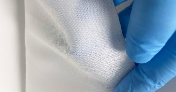
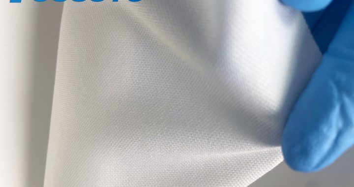
2. Ultra-Low Linting: Prevents Particle Contamination

Semiconductor equipment (especially lithography tools and wafer handlers) requires particle counts as low as ≤1 particle (≥0.1μm) per cubic foot of air. Anti-static cleanroom wipes support this by:
  • Continuous-Filament Fibers: Wipes are made from 100% polyester or polypropylene continuous filaments, not staple fibers. This eliminates fiber shedding—even under gentle wiping—unlike blended wipes that release microfibers which clog equipment vents or adhere to wafers.
  • High-Density Weave: A tight, uniform weave traps particles (down to 0.05μm) instead of pushing them across surfaces. For example, when cleaning transfer robot arms, the weave captures dust and lint that would otherwise transfer to wafers during handling, reducing yield losses from particle defects.
  • ISO Class 1–5 Certification: Reputable anti-static wipes meet ISO 14644-1 Class 1 or 5 standards, with third-party testing confirming minimal particle release. This ensures compliance with semiconductor industry norms (e.g., SEMI F21) for equipment cleaning.

3. Compatibility with Sensitive Equipment Materials

Semiconductor equipment uses specialized materials—including anti-reflective lens coatings, anodized aluminum, and delicate polymers—that can degrade with harsh cleaning tools. Anti-static cleanroom wipes address this through:
  • Non-Abrasive Construction: The soft, smooth fiber surface avoids scratching optical components (e.g., lithography lenses) or stripping protective coatings from wafer chucks. Unlike paper towels or abrasive cloths, they clean without damaging critical surfaces.
  • Residue-Free Performance: Dry anti-static wipes leave no lint or chemical residues, while pre-moistened variants use high-purity solvents (e.g., 99.9% IPA) that evaporate completely. This prevents residue buildup on equipment contacts (e.g., connector pins), which can cause electrical malfunctions or poor wafer alignment.
  • Material Compatibility Testing: Wipes undergo rigorous testing to ensure they don’t react with semiconductor equipment materials—e.g., no discoloration of anodized aluminum or degradation of polymer gaskets—making them safe for daily use on high-value tools.

4. Streamlined Cleaning Workflows

Semiconductor manufacturing demands efficiency, and anti-static cleanroom wipes boost productivity by:
  • Dual Functionality: They combine dust removal with static control in one step, eliminating the need for separate “static-neutralizing” tools (e.g., ionizers) before cleaning. This cuts cleaning time for equipment like wafer chucks by 30%.
  • Convenient Formats: Wipes are available in sizes tailored to semiconductor tasks—small 4”x4” wipes for cleaning lens edges, and larger 12”x12” wipes for robot arms—reducing waste and ensuring full surface coverage.
  • Sealed, Clean Packaging: Wipes come in airtight, anti-static packaging that keeps them contamination-free until use. This eliminates pre-cleaning steps (e.g., wiping wipes to remove dust) and ensures consistency across shifts.
For semiconductor facilities, anti-static cleanroom wipes are more than a cleaning tool—they are a critical safeguard against ESD damage and particle contamination, directly supporting higher yields, lower equipment downtime, and compliance with industry standards.

Buyer’s Guide: Anti-Static Wipes for Class 100 Cleanrooms

Class 100 cleanrooms (per ISO 14644-1, equivalent to ISO Class 5) represent the gold standard for ultra-low-contamination environments—used in semiconductor wafer fabrication (≤5nm processes), medical device manufacturing (e.g., implantable sensors), and aerospace component assembly. In these spaces, even 1 particle (≥0.5μm) per cubic foot of air or a tiny electrostatic discharge (ESD) can ruin high-value products or compromise sterile conditions. Anti-static cleanroom wipes for Class 100 environments are not just “clean”—they must meet rigorous standards for particle control, static dissipation, and material purity. This guide outlines critical criteria to ensure you select wipes that protect your processes, equipment, and products.

1. Prioritize Cleanroom Classification Compliance

Class 100 cleanrooms demand wipes certified to match their strict particle limits—never compromise on this foundational requirement:
  • ISO 14644-1 Class 5 Certification: Verify the wipe manufacturer provides third-party testing reports confirming compliance with ISO Class 5 (the international equivalent of Class 100). This ensures the wipe releases ≤10 particles (≥0.1μm) and ≤1 particle (≥0.5μm) per wipe during use—critical for avoiding particle-induced defects in semiconductors or medical devices.
  • Non-Shedding Material: Choose wipes made from ultra-low-linting substrates like 100% continuous-filament polyester or polypropylene. Avoid blended fibers (e.g., polyester-cotton) or staple-filament materials—these shed microfibers that can float in Class 100 air and contaminate surfaces. Test for linting by wiping a black, non-abrasive surface and inspecting for visible fibers under 10x magnification.

2. Validate Anti-Static Performance (Non-Negotiable for ESD-Sensitive Environments)

ESD is a silent risk in Class 100 cleanrooms—static charges can attract particles or damage ESD-sensitive components (e.g., wafer sensors, microchips). Evaluate wipes on these metrics:
  • Surface Resistance Range: Select wipes with surface resistance between 10⁶–10¹¹ Ω (per ANSI/ESD S20.20 standards). This “static-dissipative” range ensures charges are safely grounded without creating electrical arcs. Avoid “conductive” wipes (resistance <10⁶ Ω) for general use—they may cause unintended electrical pathways in delicate equipment.
  • Static Decay Time: Confirm the wipe’s static decay time (time to reduce a 5000V charge to <50V) is ≤2 seconds. Slow decay allows static to linger, increasing particle attraction. Ask manufacturers for IEC 61340-5-1 test data to validate this performance.
  • Anti-Static Treatment Durability: Ensure the anti-static coating is “permanent” (not just a surface spray). Wipes for Class 100 cleanrooms should retain their static-dissipative properties through multiple uses (if reusable) or during storage (for single-use options). Avoid wipes where anti-static efficacy degrades with humidity or time.

3. Match Wipe Type to Class 100 Cleaning Tasks

Class 100 cleanrooms require targeted cleaning—choose wipe formats and formulations based on your specific needs:
  • Dry Wipes: Ideal for removing loose, dry particles (e.g., dust on wafer chucks, lithography tool exteriors). Opt for dry wipes with a dense, smooth texture—this traps particles instead of pushing them around. Use dry wipes first before wet cleaning to avoid embedding particles into surfaces.
  • Pre-Wet Wipes: For removing oils, flux residues, or fingerprints (common in electronics manufacturing), select pre-wet wipes with high-purity solvents:
    • IPA (Isopropyl Alcohol) Wipes: Use 99.9% pure IPA (for oil-free surfaces) or 70% IPA + 30% deionized (DI) water (for better residue dissolution). Ensure the IPA is “semiconductor-grade” (≤10ppb impurities) to avoid trace chemical contamination.
    • Residue-Free Disinfectant Wipes: For sterile Class 100 environments (e.g., medical device labs), choose wipes with hydrogen peroxide (3%) or peracetic acid formulations—these disinfect without leaving toxic or particulate residues.
  • Size and Thickness: Select smaller wipes (e.g., 4”x4”) for precision tasks (e.g., cleaning around microchips) to reduce waste and avoid over-wiping. Thicker wipes (≥80gsm) offer better durability—critical for avoiding tearing (which releases particles) during use.

4. Evaluate Manufacturing and Packaging Quality

Even the best wipe material can be compromised by poor manufacturing or packaging:
  • Cleanroom-Grade Production: Ensure wipes are manufactured in an ISO Class 5 (or better) facility. This prevents pre-use contamination from the factory floor. Ask for a “Certificate of Analysis (CoA)” with each batch, detailing particle counts and static performance.
  • Sealed, Anti-Static Packaging: Wipes should arrive in airtight, static-shielding packaging (e.g., foil-lined bags with resealable zippers). Once opened, store wipes in a Class 100-compatible dispenser with a dust-tight lid—exposure to non-Class 100 air will contaminate the wipes.
  • Shelf-Life and Storage Conditions: Check the manufacturer’s shelf-life (typically 12–24 months for pre-wet wipes). Store wipes in a cool (15–25°C), dry (30–50% RH) area—extreme temperatures or humidity degrade anti-static treatments and solvent purity.

5. Avoid Common Pitfalls

  • Don’t Sacrifice Quality for Cost: Cheaper wipes may skip Class 100 certification or use low-grade materials—costly defects from contamination will far outweigh initial savings.
  • Don’t Reuse Single-Use Wipes: Single-use Class 100 wipes are designed for one pass—reusing them traps particles and degrades anti-static performance.
  • Don’t Overlook Compatibility: Test wipes on a small, non-critical surface (e.g., a spare wafer or equipment part) to ensure they don’t damage coatings (e.g., anti-reflective lens coatings) or plastics.
By following these criteria, you’ll select anti-static cleanroom wipes that not only meet Class 100 standards but also protect your high-value processes from contamination and ESD—ultimately reducing defects, minimizing downtime, and ensuring regulatory compliance.

Cleaning a Semiconductor Cleanroom with Wipes.

Semiconductor cleanrooms (typically ISO 14644-1 Class 1 to Class 5) demand ultra-stringent contamination control—even a single sub-micron particle, trace chemical residue, or electrostatic discharge (ESD) can ruin wafers, damage lithography equipment, or compromise chip performance. Traditional cleaning methods (e.g., manual solvent spraying, dry lint-free cloths) often fall short: they risk uneven solvent application, particle redistribution, or ESD. This case study details how a leading semiconductor manufacturer integrated specialized cleanroom cleaning wipes into its workflow, resolving longstanding contamination challenges and improving production efficiency.

Background: Contamination Pain Points in Wafer Processing

The manufacturer operated a Class 3 cleanroom focused on 7nm wafer fabrication—a process requiring near-absolute purity. Prior to adopting specialized cleaning wipes, the team faced two critical issues:
  1. Residue-Related Wafer Defects: After cleaning wafer chucks (the platforms holding wafers during lithography), trace residues from manual IPA (isopropyl alcohol) spraying remained. These residues (often from inconsistent solvent dilution or incomplete evaporation) caused 8–10% of wafers to fail post-processing inspections due to “stain defects” on the wafer surface.
  2. Particle Cross-Contamination: Dry lint-free cloths used to wipe equipment exteriors (e.g., lithography machine covers, transfer robot arms) shed microfibers. These fibers were detected in air sampling, leading to unscheduled cleanroom shutdowns for HEPA filter replacement—costing ~$50,000 per shutdown.
  3. ESD Risks: Standard wipes generated static charges when rubbed against stainless steel or plastic surfaces, posing a threat to ESD-sensitive components like wafer sensors. On average, 1–2 ESD-related sensor failures occurred monthly, halting production for 4–6 hours each time.

Solution: Adopting Semiconductor-Grade Cleaning Wipes

The manufacturer switched to three types of semiconductor-specific cleaning wipes, selected for their compliance with cleanroom standards and targeted performance:
Wipe Type Key Features Use Case
Pre-Wet IPA Wipes 99.9% high-purity IPA, lint-free polyester substrate, non-shedding, fast-evaporating Cleaning wafer chucks and lithography tool contact surfaces
Particle-Trapping Microfiber Wipes Ultra-fine (0.1μm) microfiber weave, static-dissipative coating (surface resistance: 10⁷–10⁹ Ω), ISO Class 1-certified Wiping equipment exteriors and transfer robot arms
Residue-Free Disinfectant Wipes Formulated with hydrogen peroxide (3%) and deionized water, non-corrosive to stainless steel/plastics Weekly deep cleaning of cleanroom workstations
All wipes were sourced from suppliers with ISO 13485 certification (medical device-grade manufacturing) to ensure batch-to-batch consistency—critical for avoiding variability in cleaning performance.

Implementation: Integrated Wiping Protocols

To maximize efficacy, the team developed a structured cleaning workflow aligned with wafer processing cycles:
  1. Pre-Lithography Chuck Cleaning: Before each wafer load, a technician uses a pre-wet IPA wipe to clean the wafer chuck in a “spiral pattern” (starting from the center and moving outward). This ensures uniform solvent coverage and eliminates residue buildup in chuck grooves. The wipe is discarded immediately after use to prevent cross-contamination.
  2. Hourly Equipment Exterior Wipes: Every hour, staff use particle-trapping microfiber wipes to clean transfer robot arms and lithography machine covers. The wipes’ static-dissipative coating eliminates charge buildup, while the microfiber weave traps particles as small as 0.3μm—no fiber shedding was detected in post-implementation air sampling.
  3. Weekly Deep Cleaning: Once weekly, the cleanroom is partially shut down for disinfection. Residue-free disinfectant wipes are used to clean workstations and tool surfaces, with no rinsing required (the formula evaporates completely within 2 minutes, leaving zero residues).

Results: Measurable Improvements in Purity and Efficiency

After 6 months of implementation, the manufacturer documented significant gains:
  • Wafer Defect Rate: Residue-related defects dropped from 8–10% to <1%, reducing wafer waste by ~90% and saving ~$200,000 monthly in material costs.
  • Particle Contamination: Air sampling showed a 95% reduction in microfiber particles, eliminating unscheduled cleanroom shutdowns—saving ~$300,000 annually in downtime costs.
  • ESD Incidents: Static-dissipative wipes reduced ESD-related sensor failures to zero, cutting production halts by 100% and improving overall equipment efficiency (OEE) by 12%.
  • Labor Efficiency: Technicians spent 30% less time on cleaning tasks (no more manual solvent mixing or re-wiping to remove residues), freeing up time for core production activities.

Long-Term Impact: Compliance and Scalability

Beyond immediate gains, the wipes helped the manufacturer maintain compliance with SEMI F21 (semiconductor equipment cleaning standards) and ISO 14644-1 Class 3 requirements—critical for securing contracts with automotive and aerospace chip clients. The team also scaled the protocol to its new 5nm wafer cleanroom, with identical performance results, proving the solution’s adaptability to advanced semiconductor processes.
This case study demonstrates that semiconductor cleanrooms require more than “general-purpose” cleaning wipes—specialized, standards-aligned wipes are a strategic investment, resolving contamination risks while driving cost savings and efficiency.