Semiconductor cleanrooms (typically ISO 14644-1 Class 1 to Class 5) demand ultra-stringent contamination control—even a single sub-micron particle, trace chemical residue, or electrostatic discharge (ESD) can ruin wafers, damage lithography equipment, or compromise chip performance. Traditional cleaning methods (e.g., manual solvent spraying, dry lint-free cloths) often fall short: they risk uneven solvent application, particle redistribution, or ESD. This case study details how a leading semiconductor manufacturer integrated specialized cleanroom cleaning wipes into its workflow, resolving longstanding contamination challenges and improving production efficiency.
Background: Contamination Pain Points in Wafer Processing
The manufacturer operated a Class 3 cleanroom focused on 7nm wafer fabrication—a process requiring near-absolute purity. Prior to adopting specialized cleaning wipes, the team faced two critical issues:
- Residue-Related Wafer Defects: After cleaning wafer chucks (the platforms holding wafers during lithography), trace residues from manual IPA (isopropyl alcohol) spraying remained. These residues (often from inconsistent solvent dilution or incomplete evaporation) caused 8–10% of wafers to fail post-processing inspections due to “stain defects” on the wafer surface.
- Particle Cross-Contamination: Dry lint-free cloths used to wipe equipment exteriors (e.g., lithography machine covers, transfer robot arms) shed microfibers. These fibers were detected in air sampling, leading to unscheduled cleanroom shutdowns for HEPA filter replacement—costing ~$50,000 per shutdown.
- ESD Risks: Standard wipes generated static charges when rubbed against stainless steel or plastic surfaces, posing a threat to ESD-sensitive components like wafer sensors. On average, 1–2 ESD-related sensor failures occurred monthly, halting production for 4–6 hours each time.
Solution: Adopting Semiconductor-Grade Cleaning Wipes
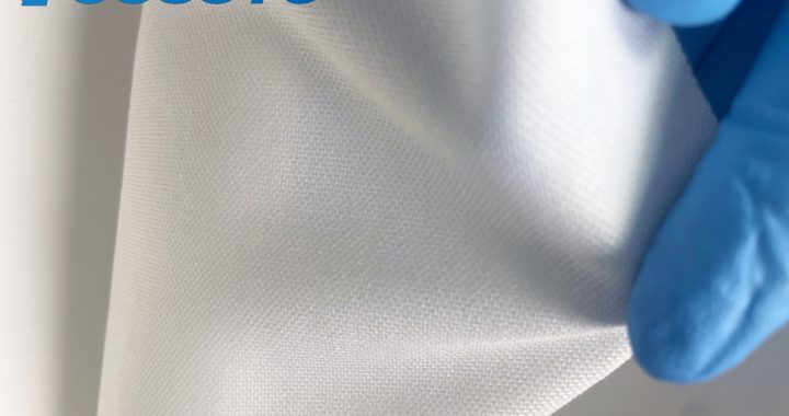
The manufacturer switched to three types of semiconductor-specific cleaning wipes, selected for their compliance with cleanroom standards and targeted performance:
| Wipe Type | Key Features | Use Case |
|---|---|---|
| Pre-Wet IPA Wipes | 99.9% high-purity IPA, lint-free polyester substrate, non-shedding, fast-evaporating | Cleaning wafer chucks and lithography tool contact surfaces |
| Particle-Trapping Microfiber Wipes | Ultra-fine (0.1μm) microfiber weave, static-dissipative coating (surface resistance: 10⁷–10⁹ Ω), ISO Class 1-certified | Wiping equipment exteriors and transfer robot arms |
| Residue-Free Disinfectant Wipes | Formulated with hydrogen peroxide (3%) and deionized water, non-corrosive to stainless steel/plastics | Weekly deep cleaning of cleanroom workstations |
All wipes were sourced from suppliers with ISO 13485 certification (medical device-grade manufacturing) to ensure batch-to-batch consistency—critical for avoiding variability in cleaning performance.
Implementation: Integrated Wiping Protocols
To maximize efficacy, the team developed a structured cleaning workflow aligned with wafer processing cycles:
- Pre-Lithography Chuck Cleaning: Before each wafer load, a technician uses a pre-wet IPA wipe to clean the wafer chuck in a “spiral pattern” (starting from the center and moving outward). This ensures uniform solvent coverage and eliminates residue buildup in chuck grooves. The wipe is discarded immediately after use to prevent cross-contamination.
- Hourly Equipment Exterior Wipes: Every hour, staff use particle-trapping microfiber wipes to clean transfer robot arms and lithography machine covers. The wipes’ static-dissipative coating eliminates charge buildup, while the microfiber weave traps particles as small as 0.3μm—no fiber shedding was detected in post-implementation air sampling.
- Weekly Deep Cleaning: Once weekly, the cleanroom is partially shut down for disinfection. Residue-free disinfectant wipes are used to clean workstations and tool surfaces, with no rinsing required (the formula evaporates completely within 2 minutes, leaving zero residues).
Results: Measurable Improvements in Purity and Efficiency
After 6 months of implementation, the manufacturer documented significant gains:
- Wafer Defect Rate: Residue-related defects dropped from 8–10% to <1%, reducing wafer waste by ~90% and saving ~$200,000 monthly in material costs.
- Particle Contamination: Air sampling showed a 95% reduction in microfiber particles, eliminating unscheduled cleanroom shutdowns—saving ~$300,000 annually in downtime costs.
- ESD Incidents: Static-dissipative wipes reduced ESD-related sensor failures to zero, cutting production halts by 100% and improving overall equipment efficiency (OEE) by 12%.
- Labor Efficiency: Technicians spent 30% less time on cleaning tasks (no more manual solvent mixing or re-wiping to remove residues), freeing up time for core production activities.
Long-Term Impact: Compliance and Scalability
Beyond immediate gains, the wipes helped the manufacturer maintain compliance with SEMI F21 (semiconductor equipment cleaning standards) and ISO 14644-1 Class 3 requirements—critical for securing contracts with automotive and aerospace chip clients. The team also scaled the protocol to its new 5nm wafer cleanroom, with identical performance results, proving the solution’s adaptability to advanced semiconductor processes.
This case study demonstrates that semiconductor cleanrooms require more than “general-purpose” cleaning wipes—specialized, standards-aligned wipes are a strategic investment, resolving contamination risks while driving cost savings and efficiency.