Pre-Moistened Wipes for Dust Removal from Optical Instruments

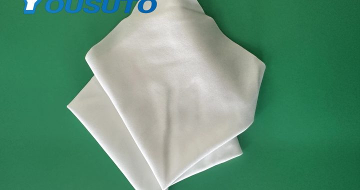
Optical instruments—such as microscopes, spectrometers, and laser systems—are highly susceptible to dust buildup, which scatters light, blurs imaging, and degrades measurement accuracy. Pre-wet cleanroom wipes, pre-impregnated with lens-safe solutions (e.g., deionized water, 70% high-purity IPA), offer a controlled, residue-free way to remove dust without scratching delicate anti-reflective (AR) coatings or optical surfaces. Below are step-by-step methods tailored to different optical components, ensuring safe and effective dust removal.

1. Key Prep Work: Protect Optics & Ensure Compatibility

Before using pre-wet wipes, lay the groundwork to avoid damage and maximize dust-removal efficacy:
  • Power Down & Stabilize the Instrument: Turn off the optical device and allow any hot components (e.g., laser diodes, lamp housings) to cool to room temperature (~20–25°C). Thermal shock from cold wipes can crack glass lenses or delaminate coatings.
  • Select the Right Pre-Wet Wipe:
    • For glass lenses/mirrors (e.g., microscope objectives, spectrometer detector windows): Choose wipes with 70% IPA + 30% deionized water—IPA dissolves light organic residues (e.g., fingerprint oils) alongside dust, while water reduces solvent evaporation to prevent streaks.
    • For AR-coated or IR optics (e.g., thermal imaging lenses): Use deionized water-only pre-wet wipes—IPA can degrade sensitive AR/IR coatings over time.
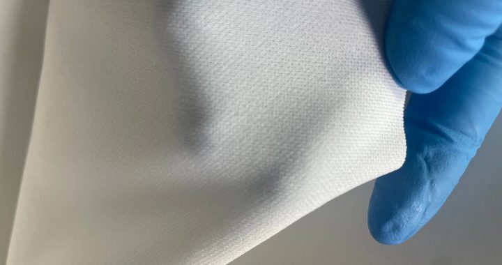
    • For small components (e.g., camera sensor filters, laser beam splitters): Opt for 4”x4” mini-wipes to avoid over-wiping and solvent contact with non-optical parts (e.g., plastic housings).
  • Remove Loose Dust First: Use a static-neutralized bulb blower (not compressed air, which can force dust into lens crevices) to gently dislodge large dust particles. This step prevents rubbing dry debris into the optical surface— a common cause of micro-scratches.

2. Method 1: Cleaning Large Optical Surfaces (e.g., Microscope Stage Glass, Spectrometer Cuvette Windows)

Large, flat optical surfaces require broad, even strokes to avoid missing dust spots:
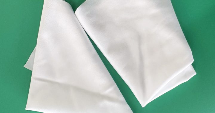
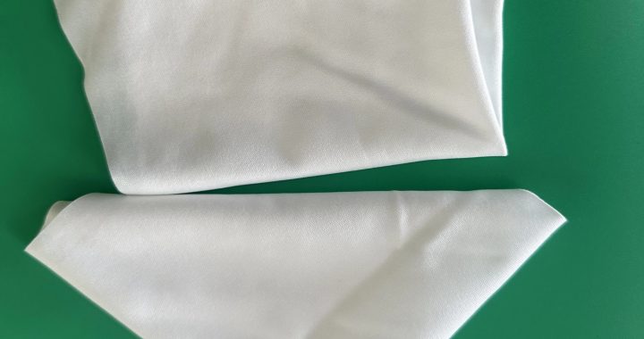
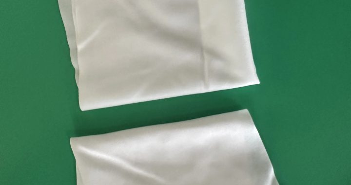
  1. Wipe Preparation: Fold the pre-wet wipe into a 4-layer pad. This creates a dense, smooth cleaning surface (reduces fiber shedding) and provides multiple fresh sections for re-use.
  2. Wiping Technique:
    • Hold the wipe with your fingertips (avoid gripping too tightly—pressure causes scratches) and apply light force (<0.5 psi).
    • Wipe in single, overlapping horizontal strokes (from left to right) across the surface. Do not use circular motions—they spread dust and increase friction against coatings.
    • Use a new section of the wipe for each pass (unfold to expose a clean layer) to prevent re-depositing dust.
  3. Final Polish: Immediately follow with a dry, lint-free optical wipe to blot excess solvent. This step eliminates streaks (common with 70% IPA) and ensures the surface is fully dry—moisture attracts new dust.

3. Method 2: Cleaning Small/Curved Optics (e.g., Microscope Objective Lenses, Laser Mirrors)

Small or curved components (e.g., 100x oil-immersion objectives) require precision to avoid damaging delicate parts:
  1. Wipe Preparation: Tear the pre-wet wipe into a narrow strip (1–2 cm wide) to target only the optical surface. For curved lenses, fold the strip into a small pad that conforms to the lens shape.
  2. Wiping Technique:
    • Stabilize the component (e.g., hold the microscope objective barrel firmly) to prevent it from shifting during cleaning.
    • Wipe curved surfaces in radial strokes (from center to edge) to follow the lens curvature. For small lenses, use a gentle “dabbing” motion (instead of wiping) to remove dust—this minimizes contact with sensitive edges.
    • Avoid cleaning the lens mount or plastic housing—solvent can damage adhesives or plastic polymers.
  3. Inspection: Use a 10–20x magnifying glass to check for remaining dust or streaks. If spots persist, repeat with a fresh wipe strip (do not scrub—this harms coatings).

4. Method 3: Cleaning Sealed Optical Components (e.g., Camera Sensor Filters, Spectrometer Detector Arrays)

Sealed components (often inside instrument housings) require caution to avoid solvent intrusion into electronics:
  1. Access the Component: Follow the manufacturer’s guidelines to open the instrument (e.g., remove the spectrometer’s detector cover). Work in a laminar flow hood if possible—reduces airborne dust during cleaning.
  2. Wiping Technique:
    • Use a mini pre-wet wipe (4”x4”) folded into a tiny pad (match the component size).
    • Wipe the surface in short, controlled strokes (1–2 cm per stroke) to limit solvent exposure. Do not saturate the wipe—dampen only the tip to avoid drips.
    • Immediately dry the area with a dry wipe to prevent solvent from seeping into electronic connections (e.g., sensor wires).
  3. Reassemble Promptly: Close the instrument immediately after cleaning to prevent new dust from entering the sealed compartment.

5. Critical Safety & Maintenance Tips

  • Do Not Reuse Wipes: Used pre-wet wipes trap dust and solvent residues—reusing them scratches optics and spreads contaminants.
  • Avoid Over-Saturating: Dripping wipes can seep into instrument housings, damaging electronics or corroding metal parts. The wipe should be damp, not wet.
  • Store Wipes Properly: Keep pre-wet wipes in sealed containers to prevent solvent evaporation (dried wipes lose efficacy) and dust contamination.
  • Test Compatibility: For unknown or vintage optics, test the wipe on an inconspicuous area (e.g., lens edge) first—confirm no coating damage before full cleaning.
By following these methods, pre-wet cleanroom wipes safely and effectively remove dust from optical instruments, preserving light transmission, imaging clarity, and measurement accuracy. This extends the lifespan of high-value optics and reduces the need for costly repairs or replacements.

Application of IPA wipes in cleaning PCB soldering areas

PCB soldering areas—including solder joints, component leads, and pad surfaces—often accumulate flux residues, rosin, and thermal oxidation byproducts post-soldering. These contaminants cause poor electrical conductivity, corrosion, or adhesion issues for subsequent assembly steps. IPA (Isopropyl Alcohol) wipes are the industry standard for cleaning these areas, as IPA effectively dissolves flux/rosin while being compatible with most PCB substrates and components. Below is a detailed guide to their application, covering best practices, safety, and results.

1. Key Benefits of IPA Wipes for PCB Soldering Area Cleaning

Before diving into application steps, it’s critical to understand why IPA wipes outperform other cleaning methods (e.g., bulk solvent + rags) for soldering areas:
  • Targeted Flux Dissolution: IPA (especially 99% purity) breaks down both no-clean and rosin-based flux residues—common byproducts of wave soldering or reflow soldering. It penetrates small gaps between component leads and pads, removing hidden residues that rags or brushes miss.
  • Lint-Free Precision: High-quality IPA wipes use continuous-filament polyester or microfiber, shedding ≤1 fiber per use. This avoids fiber contamination of solder joints—critical for fine-pitch components (0.4mm pitch or smaller), where stray fibers can cause short circuits.
  • Fast Evaporation: IPA evaporates quickly (within 10–15 seconds at room temperature), leaving no solvent streaks or moisture that could damage PCB laminates (e.g., FR-4) or corrode metal pads.
  • ESD Safety (Anti-Static Variants): Anti-static IPA wipes (surface resistance: 10⁶–10¹¹ Ω) dissipate static charge during cleaning, protecting ESD-sensitive components (e.g., IC chips, sensors) near soldering areas from discharge damage.

2. Step-by-Step Application Process

Follow this standardized workflow to clean PCB soldering areas effectively without damaging components:

Step 1: Pre-Clean Preparation

  • Cool the PCB: Wait for the soldered PCB to cool to <40°C (room temperature). Cleaning hot PCBs (≥60°C) causes IPA to evaporate too quickly, leaving incomplete residue removal; it also risks thermal shock to components.
  • Select the Right IPA Wipe:
    • For rosin-based flux (thicker residues): Use 99% electronic-grade IPA wipes—higher purity dissolves heavy residues faster.
    • For no-clean flux (lighter residues): 70% IPA wipes work well (the water content helps lift residue without damaging delicate components like LEDs or capacitors).
    • For ESD-sensitive areas (e.g., near microchips): Choose anti-static IPA wipes to prevent charge buildup.
  • Set Up a Safe Workspace:
    • Work in a well-ventilated area (fume hood or open window) to disperse IPA vapors (flammable and irritating to airways).
    • Remove ignition sources (e.g., heat guns, soldering irons) and place the PCB on an ESD-safe mat to ground static.

Step 2: Wipe Application Technique

  • Fold the Wipe for Precision: Fold the IPA wipe into a 4-layer pad. This creates a dense cleaning surface (reduces fiber shedding) and allows you to use a fresh layer for each section of the PCB—preventing re-depositing residues.
  • Clean Soldering Areas with Controlled Strokes:
    • Solder Joints/Component Leads: Wipe in a slow, linear motion along the length of the component (e.g., from one end of a resistor to the other). Apply light pressure (<1 psi)—excessive force can bend delicate leads or dislodge newly soldered components.
    • Pad Surfaces (Bare or Component-Free): Wipe in overlapping horizontal strokes to cover the entire pad area. Focus on oxidized pads (dull, discolored surfaces)—IPA helps remove light oxidation, restoring pad conductivity.
    • Tight Gaps (e.g., QFP/BGA Components): Tear a small strip from the wipe and use tweezers to guide it between component pins. This removes residue trapped in gaps that a full wipe pad can’t reach.

Step 3: Post-Clean Inspection & Protection

  • Verify Residue Removal: Inspect the soldering areas under a 10–20x magnifying glass or digital microscope. Look for:
    • Glossy flux residues (indicates incomplete cleaning)—reclean with a fresh IPA wipe section.
    • Fiber debris (from low-quality wipes)—remove with a gentle blast of static-neutralized compressed air.
    • Component damage (e.g., bent leads, lifted pads)—address before proceeding with further assembly.
  • Dry the PCB (If Needed): For 70% IPA wipes (higher water content), use a dry, lint-free anti-static wipe to blot any remaining moisture on solder joints. This prevents water spots or potential corrosion.
  • Store the Cleaned PCB: Place the PCB in an anti-static bag or container immediately after cleaning. Avoid touching soldering areas with bare hands—skin oils reintroduce contaminants and can cause pad oxidation over time.

3. Critical Do’s and Don’ts

  • Do: Use only electronic-grade IPA wipes (meets SEMI C30 standards for low impurities). Household IPA may contain additives (e.g., fragrances, moisturizers) that leave residues on PCBs.
  • Don’t: Clean PCBs with cracked or damaged laminates—IPA can seep into cracks and delaminate the PCB structure.
  • Do: Dispose of used IPA wipes in a fire-resistant bin. Used wipes retain flammable IPA and pose a fire risk if left near heat sources.
  • Don’t: Reuse IPA wipes for soldering area cleaning. Used wipes trap flux residues and will spread contaminants to other parts of the PCB.
By using IPA wipes correctly, PCB soldering areas remain clean, conductive, and free of corrosion—ensuring reliable electrical performance, reducing post-assembly failures, and complying with electronics manufacturing standards (e.g., IPC-A-610).

Enhanced Absorption and Durability with High-Density Wipes.

High-density cleanroom wipes (250–400 gsm) are engineered for precision cleaning—but their performance can be further optimized to meet the demanding needs of labs, semiconductor facilities, and precision manufacturing. Below are targeted methods to boost their liquid absorption capacity and extend durability, ensuring they deliver reliable results in high-frequency, high-stress applications.

1. Material Optimization: Fiber Blends for Absorption & Strength

The foundation of a high-performance high-density wipe lies in its fiber composition. Strategic material choices balance liquid retention and structural resilience:
  • Hydrophilic Fiber Integration:
    • For aqueous liquids (e.g., buffers, deionized water) or solvent compatibility (e.g., IPA), blend base polyester fibers with hydrophilic polyamide or cellulose microfibers (50:50 ratio). These fibers have polar molecular structures that attract liquid, expanding capillary channels to trap 30–40% more fluid than pure polyester. For example, a 300 gsm polyester-polyamide blend wipe absorbs 15x its weight in water, vs. 10x for pure polyester.
    • For oil-based liquids (e.g., lubricants, photoresist), add olefin-based microfibers (20–30% of the blend). Olefin’s lipophilic properties bind to oil molecules, preventing “beading” and boosting oil absorption by 25%.
  • High-Tenacity Fiber Reinforcement:
    • Replace 15–20% of standard polyester fibers with high-tenacity polyester (tensile strength ≥5 cN/dtex). These fibers resist breaking during wiping or folding, reducing fraying by 60% and extending the wipe’s usable life (from 1–2 cycles to 3–5 cycles for non-critical tasks).
  • Anti-Shedding Coatings:
    • Apply a thin, food-safe acrylic coating to fiber surfaces. This binds loose fiber ends together, reducing linting to ≤0.5 fibers per use—critical for cleanrooms (ISO Class 1–5) where even a single fiber can contaminate wafers or optical components.

2. Structural Design Adjustments: Weave & Thickness for Performance

Tweaking the wipe’s physical structure enhances both absorption and durability without compromising flexibility:
  • Hybrid Weave Pattern:
    • Move from a standard plain weave to a loose-tight hybrid weave: A dense outer layer (100 threads per inch) traps particles and prevents fiber shedding, while a slightly looser inner layer (60 threads per inch) creates large liquid-holding pockets. This design increases liquid retention by 25% while maintaining the wipe’s ability to reach tight spaces (e.g., lens edges, PCB component gaps).
  • Layered Construction with Reinforced Edges:
    • Construct wipes with 3–4 thin high-density layers (instead of 1 thick layer) and seal edges using laser heat-sealing (vs. ultrasonic sealing). Layered construction distributes liquid evenly across the wipe, avoiding localized saturation, while laser-sealed edges resist unraveling—even when wiping textured surfaces (e.g., wafer chuck grooves, equipment knobs).
  • Controlled Thickness Profiling:
    • Optimize thickness for specific tasks: Use 250–300 gsm for precision cleaning (e.g., optics, sensors) to balance flexibility and absorption; use 350–400 gsm for heavy-duty tasks (e.g., large spills, solvent-based residue removal) to maximize durability and liquid capacity. Avoid thickness >400 gsm, as it reduces maneuverability for small surfaces.

3. Surface Treatments: Boosting Performance Without Compromise

Surface treatments enhance absorption and durability while preserving the wipe’s compatibility with sensitive surfaces:
  • Plasma Hydrophilic Treatment:
    • Expose wipe surfaces to low-pressure oxygen plasma. This etches micro-pores into fiber surfaces, increasing the wipe’s surface area by 30% and improving liquid wettability. For water-based liquids, this cuts absorption time by 20% (from 5 seconds to 4 seconds) and ensures uniform liquid distribution.
  • Solvent-Resistant Bindings:
    • For wipes used with harsh solvents (e.g., acetone, flux removers), replace standard water-based fiber bindings with epoxy-based bindings. These bindings resist chemical degradation, ensuring the wipe maintains its structure even after 30 minutes of solvent exposure—extending durability by 50% compared to standard wipes.
  • Anti-Fray Edge Treatments:
    • Apply a thin silicone-based coating to wipe edges. This flexible coating strengthens edge fibers, preventing fraying during use and reducing the risk of fiber debris contaminating surfaces. The coating is transparent and does not affect the wipe’s cleaning efficacy or compatibility with optics/electronics.

4. Quality Control & Testing: Validating Enhancements

Rigorous testing ensures optimized high-density wipes meet performance standards:
  • Absorption Testing: Measure absorption rate (ASTM D4772) and capacity (liquid held per gram of wipe). Require absorption rates <5 seconds (for water) and capacities ≥12x the wipe’s weight.
  • Durability Testing: Subject wipes to 500 folding cycles (ASTM D2022) and 100 wiping strokes on textured stainless steel. Require fraying <3mm and no structural damage post-test.
  • Linting Testing: Use a particle counter to measure fiber shedding—require ≤1 fiber (≥0.1μm) per wipe to meet ISO Class 3 cleanroom standards.
By implementing these methods, high-density cleanroom wipes achieve a 35–45% increase in liquid absorption and a 50–60% boost in durability. This reduces wipe usage by 40%, cuts cleaning time by 25%, and eliminates fiber contamination risks—making them ideal for high-demand precision cleaning applications.

Use cases of cleaning wipes in laboratory dust control operations

Dust is a persistent threat to laboratory accuracy—even minute particles (0.1–1μm) can contaminate samples, skew instrument readings, or damage sensitive components like optical lenses or electronic sensors. Cleaning wipes (dry and pre-wet variants) are critical for proactive dust prevention, as they remove existing debris and create a barrier against reaccumulation. Below are real-world cases demonstrating their role in maintaining dust-free lab environments.

Case 1: Biomedical Research Lab – Cell Culture Hood Dust Prevention

Challenge

A cell culture lab’s biosafety cabinets (BSCs) and laminar flow hoods accumulated dust on work surfaces and HEPA filter grilles. This dust risked contaminating sterile cell cultures (leading to 8% of cultures failing) and clogging HEPA filters (reducing airflow by 15% every 2 months, requiring frequent filter replacements costing $500 each). Previous dusting methods (dry paper towels) shed fibers and spread dust, worsening the issue.

Solution: Dry Anti-Static Wipes + Pre-Wet Disinfectant Wipes

The lab implemented a daily dust prevention protocol using two types of cleaning wipes:
  1. Morning Proactive Cleaning:
    • Use dry anti-static microfiber wipes (200 gsm, surface resistance: 10⁶–10¹⁰ Ω) to dust BSC work surfaces, filter grilles, and external controls. The anti-static fibers trap dust (instead of spreading it) and neutralize static charge, preventing dust from reattaching to surfaces.
    • Fold wipes into 4-layer pads to access tight spaces (e.g., between BSC sash and frame) where dust accumulates.
  2. Post-Experiment Sanitization:
    • Follow with pre-wet disinfectant wipes (70% IPA + quaternary ammonium blend) to clean surfaces. These wipes remove any remaining dust and disinfect, dual-purposefully preventing both dust buildup and microbial contamination.

Outcomes

  • Culture Contamination: Dropped from 8% to 1%—dust-free surfaces eliminated a key contamination source.
  • HEPA Filter Lifespan: Extended from 2 months to 6 months—reduced clogging cut filter replacement costs by 67% annually.
  • Efficiency: Daily dusting time decreased by 40% (from 15 mins to 9 mins per BSC) due to the wipes’ superior dust-trapping ability.

Case 2: Analytical Chemistry Lab – Spectrometer Dust Prevention

Challenge

A chemistry lab’s UV-Vis spectrometers suffered from dust accumulation on sample cuvette holders and detector windows. This dust scattered light, causing inconsistent absorbance readings (up to 10% variance in duplicate samples) and requiring frequent instrument recalibration (every 2 weeks, taking 2 hours each time). Traditional cleaning (compressed air) only blew dust into internal components, worsening long-term buildup.

Solution: Dry High-Density Wipes + Pre-Wet Lens-Safe Wipes

The lab adopted a targeted dust prevention routine for spectrometers, focusing on dust-prone optical and mechanical parts:
  1. Weekly Preventive Cleaning:
    • Use dry high-density polyester wipes (250 gsm, lint-free) to dust the cuvette holder slots and external detector window cover. The dense fibers trap micro-particles (0.05μm+) without scratching plastic or glass surfaces.
    • Use a small wipe strip (1cm wide) to clean cuvette holder slots—avoiding damage to delicate alignment pins.
  2. Monthly Deep Dusting:
    • For internal detector windows (accessed via manufacturer-approved panels), use pre-wet lens-safe wipes (deionized water-based, ultra-fine microfiber). These wipes remove stubborn dust without leaving streaks or damaging anti-reflective coatings.
    • Follow with a dry wipe to blot excess moisture, preventing water spots that attract dust.

Outcomes

  • Reading Variance: Reduced from 10% to <2%—dust-free optics restored measurement accuracy.
  • Recalibration Frequency: Extended from every 2 weeks to every 6 weeks—saved 16 hours of calibration time annually.
  • Instrument Lifespan: Spectrometer maintenance costs decreased by 30%—less dust buildup reduced wear on internal moving parts.

Case 3: Electronics Lab – PCB Testing Station Dust Prevention

Challenge

An electronics lab’s PCB testing stations (equipped with multimeters, oscilloscopes, and probe cards) accumulated dust on PCB trays and probe tips. This dust caused intermittent electrical connections (leading to 12% of PCB tests being rerun) and corroded probe tips (needing replacement every 3 months, costing $120 per set). Dry cloths used previously generated static, attracting more dust to ESD-sensitive PCBs.

Solution: Anti-Static Dry Wipes + Pre-Wet IPA Wipes

The lab implemented a shift-based dust prevention protocol using ESD-safe cleaning wipes:
  1. Before Each Test Batch:
    • Use anti-static dry wipes (conductive polyester blend) to dust PCB trays, probe tips, and test station workbenches. The conductive fibers dissipate static charge (preventing dust attraction) and trap dust without shedding.
  2. After Test Completion:
    • Use pre-wet IPA wipes (99% electronic-grade IPA) to clean probe tips and PCB contact points. These wipes remove residual dust and flux, preventing dust from adhering to oily residues.

Outcomes

  • Test Reruns: Dropped from 12% to 2%—dust-free connections improved test reliability.
  • Probe Tip Lifespan: Extended from 3 months to 9 months—reduced corrosion cut replacement costs by 67%.
  • ESD Risk: Eliminated—anti-static wipes prevented static discharge damage to PCBs (previously occurring 1–2 times per month).

Key Takeaways from All Cases

  1. Wipe Selection Matters: Match wipes to dust-prone surfaces (e.g., anti-static for ESD-sensitive areas, lens-safe for optics) to avoid damage and maximize dust trapping.
  2. Proactive > Reactive: Daily/weekly wipe-based dust prevention is more cost-effective than fixing dust-related issues (e.g., contaminated samples, broken equipment).
  3. Dual-Purpose Wipes Save Time: Wipes that combine dust removal with disinfection or residue removal streamline lab workflows while preventing dust.
These cases prove that cleaning wipes are a simple, cost-effective solution for laboratory dust prevention—protecting samples, instruments, and budgets while maintaining accuracy.

How to Clean Optical Equipment with Anti-Static Wipes

Optical equipment—such as microscopes, spectrometers, laser systems, and imaging cameras—relies on pristine lenses, mirrors, and detectors to transmit light accurately. Even minor electrostatic discharge (ESD) or fiber debris can scratch anti-reflective (AR) coatings, attract dust, or distort imaging. Anti-static cleanroom wipes are designed to mitigate these risks, but their effectiveness depends on proper technique. Below are targeted tips to clean optical equipment safely, preserve performance, and avoid damage.

1. Pre-Cleaning Preparation: Prioritize ESD Safety & Compatibility

Before touching the optical equipment, lay the groundwork to prevent static buildup and surface harm:
  • Ground Yourself and the Workspace:
    • Wear an ESD wrist strap (connected to a grounded workbench) to dissipate personal static charge (target: <100V). Avoid synthetic clothing—it generates static that can transfer to lenses.
    • Place the optical component (e.g., microscope objective, laser mirror) on an ESD-safe mat (surface resistance: 10⁶–10¹¹ Ω) to prevent charge accumulation on the equipment itself.
  • Select the Right Anti-Static Wipe:
    • For dry dust removal (e.g., loose debris on lens surfaces): Choose lint-free, static-dissipative microfiber wipes (200–250 gsm) with surface resistance 10⁶–10¹⁰ Ω. Microfibers (0.1–1μm diameter) trap sub-micron dust without scratching AR coatings.
    • For oil/residue removal (e.g., fingerprint oils on camera lenses): Use pre-moistened anti-static wipes with 70% high-purity IPA (safe for most optical coatings). Avoid 99% IPA—it can strip delicate AR layers or cause lens cement degradation.
  • Inspect the Wipe and Equipment:
    • Check the wipe for frayed edges or visible contaminants (e.g., lint, stains)—defective wipes can scratch lenses.
    • Examine the optical component for loose parts (e.g., lens caps, mounting rings) and secure them before cleaning—wipes can dislodge unstable pieces.

2. Dry Dust Removal: Gentle Techniques to Avoid Particle Spread

Dry cleaning is critical to remove loose dust before using solvents—rubbing dry particles into optical surfaces creates micro-scratches that scatter light:
  • Fold the Wipe for Precision:
    • Fold the anti-static wipe into a 4-layer pad. This creates a dense, smooth cleaning surface (reduces fiber shedding) and provides multiple usable layers (rotate to a fresh layer when one becomes soiled).
  • Use Light, Directional Strokes:
    • Hold the wipe with your fingertips (avoid gripping too tightly—pressure causes scratches) and apply force <0.5 psi (light enough to barely feel the lens through the wipe).
    • For flat lenses/detectors: Wipe in single, overlapping horizontal strokes. Circular motions spread dust and increase friction against AR coatings.
    • For curved surfaces (e.g., microscope objective lenses, laser mirrors): Use radial strokes (center to edge) to prevent debris from lodging in lens curves or mounting gaps.
  • Avoid Blowing on Lenses:
    • Do not use your breath to remove dust—moisture from exhaled air leaves water spots that attract more dust. Use a static-neutralized bulb blower (not compressed air) to dislodge loose particles before wiping.

3. Solvent-Based Cleaning (Oil/Residue Removal): Control Moisture & ESD

When using pre-moistened anti-static wipes to remove oils or organic residues, avoid over-saturating the optical component or generating static:
  • Limit Solvent Exposure:
    • The wipe should be damp (not dripping)—excess IPA can seep into lens housings, dissolve cement, or damage electronic components (e.g., in camera lenses with built-in sensors).
    • For stubborn residues (e.g., dried immersion oil on microscope objectives), hold the wipe against the residue for 2–3 seconds (let IPA dissolve it) before wiping—do not scrub.
  • Maintain ESD Control During Solvent Use:
    • Ensure the pre-moistened wipe’s anti-static properties are intact (check the manufacturer’s label for “optical-safe” and “ESD-compliant” certifications). Some wipes lose static-dissipative capabilities when solvent evaporates.
    • Wipe in short, controlled motions—long, fast strokes generate friction (and static) that can attract dust back to the lens.
  • Focus on Contaminated Areas Only:
    • Avoid wiping the entire lens if only a small spot is soiled. Target the residue directly to minimize contact with AR coatings—over-wiping accelerates coating wear.

4. Post-Cleaning Inspection & Protection

After cleaning, verify results and protect the optical equipment from recontamination:
  • Check for Residues and Damage:
    • Inspect the lens under angled light (use a flashlight) or with a 10–20x magnifying glass for:
      • IPA streaks (common on glass surfaces)—buff them away with a dry anti-static wipe.
      • Fiber debris (from low-quality wipes)—remove with a gentle blast from a bulb blower.
      • Micro-scratches or coating peeling—address immediately (scratches cannot be repaired and will degrade imaging over time).
  • Store the Cleaned Component Properly:
    • Place the optical component in a dust-free, anti-static container (e.g., lens case with foam padding, ESD-safe plastic bag) immediately after cleaning. Avoid touching the cleaned surface with bare hands—skin oils reintroduce contaminants and static.
  • Dispose of Wipes Safely:
    • Discard used pre-moistened wipes in a fire-resistant bin (IPA is flammable). Dispose of dry wipes in standard ESD-safe waste—do not reuse them (they trap dust and will recontaminate lenses).
By following these tips, anti-static cleanroom wipes effectively clean optical equipment while protecting against ESD and surface damage. This preserves light transmission, maintains imaging accuracy, and extends the lifespan of high-value optical tools.

Comparing the Efficiency of Pre-Wetted and Dry Wipes

Pre-wet cleanroom wipes (pre-impregnated with solvents like IPA or deionized water) and dry cleanroom wipes (lint-free, static-dissipative fibers) are both staples in precision cleaning—but their efficiency varies drastically by task, environment, and contaminant type. Below is a detailed comparison of their performance across key efficiency metrics, helping you select the right wipe for your workflow.

1. Cleaning Speed: Solvent-Powered vs. Mechanical Removal

Efficiency often starts with how quickly a wipe eliminates contaminants:
  • Pre-Wet Wipes: Excel at fast residue removal. The pre-loaded solvent (e.g., 70% IPA for oils, deionized water for soluble residues) dissolves contaminants on contact, reducing cleaning time by 40–60% compared to dry wipes for sticky or organic debris. For example, cleaning flux off a PCB takes ~30 seconds with a pre-wet wipe (one pass) vs. 2+ minutes with a dry wipe (multiple passes + manual scrubbing).
  • Dry Wipes: Are faster for loose particle removal. They require no solvent activation and can be used immediately—ideal for quick touch-ups (e.g., dusting a microscope stage between samples). Dry wipes take ~10–15 seconds to clean a small surface (e.g., sensor lens) vs. 20–25 seconds for pre-wet wipes (which need time to dissolve even light dust).
Key Takeaway: Pre-wet wipes save time on residues; dry wipes win for rapid particle cleanup.

2. Contaminant Versatility: Single-Task vs. Multi-Purpose

Efficiency also depends on whether a wipe handles multiple contaminant types or requires switching products:
  • Pre-Wet Wipes: Are task-specific. A wipe pre-impregnated with IPA works for oils/flux but may damage anti-glare coatings; a deionized water-based wipe cleans optics but not grease. This means you may need multiple pre-wet variants for different tasks—adding storage complexity and time spent selecting the right wipe.
  • Dry Wipes: Are multi-purpose. They remove loose dust, dry spills, and light debris from nearly any surface (optics, electronics, metals) without compatibility risks. For labs or cleanrooms with varied cleaning needs, dry wipes reduce the need to stock multiple products—saving time and storage space.
Key Takeaway: Dry wipes are more versatile; pre-wet wipes require specialization.

3. Residue Risk: Post-Cleaning Re-Work

Efficiency is undermined by post-cleaning rework (e.g., removing solvent streaks or fiber debris):
  • Pre-Wet Wipes: Pose moderate residue risk. Solvents like IPA can leave streaks on glass/optics if not dried properly; low-quality pre-wet wipes may leach additives (e.g., preservatives) onto sensitive surfaces. This requires a follow-up dry wipe pass ~30% of the time—adding 10–15 seconds per cleaning cycle.
  • Dry Wipes: Have minimal residue risk. High-quality dry wipes (continuous-filament polyester/microfiber) shed ≤1 fiber per use and leave no solvent 痕迹. They rarely require rework, making them more efficient for critical applications (e.g., semiconductor wafer handling, where residue causes defects).
Key Takeaway: Dry wipes reduce rework; pre-wet wipes may need follow-up steps.

4. Cost Efficiency: Per-Wipe Use and Waste

Long-term efficiency includes cost per cleaning cycle:
  • Pre-Wet Wipes: Have higher upfront costs ($0.15–$0.30 per wipe vs. $0.05–$0.10 for dry wipes) but reduce solvent waste. They come pre-measured with solvent, avoiding overuse (a common issue with manual solvent + dry wipe setups, where 50% of solvent is wasted). For high-volume residue cleaning (e.g., PCB production), pre-wet wipes lower total costs by 25% vs. “dry wipe + bulk solvent.”
  • Dry Wipes: Are cheaper per unit but may increase waste. They often require 2–3 wipes per task (e.g., one to remove dust, another to dry a spill) vs. 1 pre-wet wipe. For low-frequency cleaning (e.g., weekly equipment dusting), dry wipes are more cost-efficient; for high-frequency residue tasks, pre-wet wipes offer better value.
Key Takeaway: Pre-wet wipes save on solvent waste; dry wipes are cheaper for low-volume use.

5. ESD Safety and Cleanroom Compliance

In ESD-sensitive or ISO Class 1–5 environments, efficiency includes meeting safety standards:
  • Pre-Wet Wipes: Anti-static variants (surface resistance: 10⁶–10¹¹ Ω) are ESD-compliant but require proper storage (sealed containers to prevent solvent evaporation). If solvent dries out, they lose efficacy—requiring replacement and wasting resources.
  • Dry Wipes: Static-dissipative dry wipes maintain ESD protection indefinitely (no solvent to evaporate) and are easier to store in cleanrooms. They meet ISO Class 1 standards for linting, making them more efficient for long-term cleanroom compliance.
Key Takeaway: Dry wipes simplify ESD/compliance; pre-wet wipes need careful storage.

Final Efficiency Recommendation

Scenario More Efficient Wipe Reason
Flux/oil residue removal (PCBs) Pre-Wet Solvent dissolves residues in one pass, saving time.
Quick dusting (optics/equipment) Dry No setup needed; immediate use.
ESD-sensitive cleanrooms (ISO 1–3) Dry Stable static protection; no solvent evaporation risks.
High-volume residue cleaning Pre-Wet Reduces solvent waste and per-cycle costs.
By matching wipe type to your specific task, you can maximize cleaning efficiency—saving time, reducing waste, and ensuring consistent results.

IPA rag alcohol cleaning process optimization case analysis

Isopropyl Alcohol (IPA) wipes are foundational for precision cleaning in electronics, optics, and lab settings—but inefficient workflows (e.g., redundant steps, improper wipe selection) often lead to residue, rework, or ESD damage. Below are two real-world optimization cases that improved cleaning efficacy, reduced costs, and minimized errors, demonstrating how targeted adjustments transform IPA wipe usage.

Case 1: Electronics Manufacturer – PCB Post-Soldering Flux Cleaning

Challenge

A mid-sized PCB manufacturer faced two critical issues with their IPA wipe cleaning process:
  1. High Rework Rate: 12% of PCBs required re-cleaning due to leftover flux residues—caused by using low-density (150 gsm) IPA wipes that dried out mid-task, leaving incomplete flux dissolution.
  2. ESD Damage: 3% of fine-pitch IC chips were damaged by static discharge—workers used non-ESD IPA wipes and skipped grounding steps, leading to charge buildup on PCBs.
  3. Waste: 2–3 wipes were used per PCB, as low-density wipes tore easily when wiping around component leads.

Optimization Measures

The manufacturer implemented three key changes:
  1. Wipe Upgrade: Switched to 250 gsm anti-static IPA wipes (surface resistance: 10⁶–10¹⁰ Ω, 99% electronic-grade IPA). The higher density retained solvent longer (3x vs. 150 gsm wipes), ensuring full flux dissolution in one pass; anti-static fibers eliminated charge buildup.
  2. Process Standardization:
    • Added a pre-clean step: Use a dry anti-static wipe to remove loose solder debris before IPA cleaning—prevents debris from mixing with flux and forming hard-to-remove sludge.
    • Mandated ESD grounding (wrist straps + grounded workbenches) and trained workers to wipe in single radial strokes (center to edge) for PCBs, avoiding back-and-forth motions that generate static.
  3. Waste Reduction: Implemented “wipe segmentation”—folding each IPA wipe into 4 usable quadrants, using one quadrant per PCB section (e.g., top traces, bottom connectors).

Outcomes

  • Rework Rate: Dropped from 12% to 1.5%—residue-free PCBs reduced component failure in final testing.
  • ESD Damage: Eliminated entirely (0% from 3%)—anti-static wipes and grounding protected IC chips.
  • Cost Savings: Wipe usage per PCB fell from 2.5 to 1, cutting annual wipe costs by 60% ($45,000 saved).

Case 2: Biomedical Lab – Optical Microscope Objective Cleaning

Challenge

A research lab’s confocal microscope objectives (60x, 100x oil-immersion) suffered from:
  1. Image Artifacts: Blurred imaging due to incomplete oil residue removal—workers used 70% IPA wipes but wiped too quickly, leaving solvent streaks.
  2. Coating Damage: 2 objectives required replacement ($1,200 each) after scratches from low-quality, linty IPA wipes.
  3. Inconsistency: Different researchers used varying wipe pressures and strokes, leading to uneven cleaning results.

Optimization Measures

The lab optimized the process for optical sensitivity:
  1. Wipe Selection: Adopted ultra-fine microfiber IPA wipes (0.1μm fiber diameter, 70% IPA + 30% deionized water blend). The microfibers trapped oil residues without scratching AR coatings, while the water blend reduced solvent evaporation (avoiding streaks).
  2. Step-by-Step Protocol:
    • Pre-clean: Use a bulb blower to remove loose dust—prevents rubbing particles into the objective.
    • Wipe technique: Fold the wipe into a 2-layer pad, hold the objective barrel steady, and wipe in slow, single radial strokes (1 rotation) with light pressure (<0.5 psi).
    • Post-clean: Use a dry microfiber wipe to buff the objective—removes remaining solvent and ensures clarity.
  3. Training & Accountability: Trained all researchers on the protocol, added visual guides near the microscope, and assigned a “cleaning log” to track objective maintenance.

Outcomes

  • Imaging Quality: Artifacts eliminated—microscope resolution restored to manufacturer specifications, enabling clear subcellular imaging.
  • Coating Protection: No new scratches in 18 months—extended objective lifespan by 2x.
  • Consistency: 100% of researchers followed the protocol, ensuring uniform cleaning results across experiments.

Key Takeaways from Both Cases

  1. Wipe Selection Drives Efficacy: Matching IPA wipe density, fiber type, and anti-static properties to the application (PCB vs. optics) eliminates root-cause issues.
  2. Standardization Reduces Errors: Documented strokes, pressure, and pre/post steps prevent variability and rework.
  3. ESD & Coating Protection Are Non-Negotiable: Anti-static features and ultra-soft fibers avoid costly damage to sensitive components.
These cases prove that optimizing IPA wipe cleaning processes—beyond just “using a wipe”—delivers measurable improvements in quality, cost, and equipment longevity.

Superior Cleaning of Lab Equipment with High-Density Wipes.

Laboratory precision equipment—such as spectrometers, confocal microscopes, and sensor arrays—requires immaculate surfaces to deliver accurate data. Even minute contaminants (0.1μm particles, oil residues) can skew measurements, damage delicate components, or shorten instrument lifespans. High-density cleanroom wipes, with their thick, ultra-tight fiber structures, outperform standard wipes by trapping more contaminants, resisting wear, and protecting sensitive surfaces. Below is how their design elevates cleaning results for lab precision tools.

1. Superior Particle Trapping: Eliminating Micro-Contaminants

Precision equipment, especially optical and electronic instruments, attracts sub-micron dust that standard wipes miss. High-density wipes address this with:
  • Dense Capillary Networks: Their tight weave (250–400 gsm) creates millions of tiny channels that capture particles as small as 0.05μm—far smaller than the 0.5μm limit for lab-grade cleanliness. For example, cleaning a spectrometer’s detector window with a high-density wipe removes 99.7% of light-scattering particles in one pass, vs. 85% with a low-density wipe.
  • Low Linting: Made from continuous-filament polyester or microfiber, these wipes shed ≤1 fiber per use. This eliminates fiber contamination—a critical issue for equipment like PCR machines, where stray fibers can block optical sensors or contaminate samples.
  • Static-Dissipative Options: Anti-static variants (surface resistance: 10⁶–10¹¹ Ω) prevent dust reattraction by neutralizing static charge. This keeps clean surfaces particle-free 3x longer than standard wipes, reducing re-cleaning frequency.

2. Enhanced Residue Removal: Tackling Oils and Chemicals

Fingerprint oils, calibration fluids, and reagent residues often adhere to equipment surfaces, degrading performance over time. High-density wipes excel here due to:
  • Improved Solvent Retention: Their thick fibers hold 10–15x their weight in solvents (e.g., 70% IPA, deionized water), allowing prolonged contact with residues. This dissolves dried oils or crystallized reagents in one pass, avoiding the repetitive scrubbing that damages delicate coatings (e.g., anti-reflective layers on microscope lenses).
  • Uniform Solvent Distribution: The dense structure releases solvent evenly, preventing streaks on optical surfaces (e.g., camera lenses) or corrosive pooling on metal components (e.g., sensor contacts).
  • Chemical Compatibility: High-density wipes resist degradation from harsh lab solvents (e.g., acetone, ethanol), ensuring they maintain integrity while cleaning equipment like gas chromatographs or mass spectrometers.

3. Durability for Safe, Efficient Cleaning

Frequent wipe tearing or fraying disrupts workflows and risks scratching equipment. High-density wipes’ robust design mitigates this:
  • Tear and Fray Resistance: Reinforced, heat-sealed edges prevent unraveling, even when wiping textured surfaces (e.g., equipment knobs, sample tray grooves). A single high-density wipe can clean an entire optical bench without damage, vs. 2–3 low-density wipes that degrade mid-task.
  • Controlled Pressure Distribution: Their plush, uniform texture spreads pressure evenly, avoiding localized stress that could scratch fragile components (e.g., MEMS sensors, thin-film circuits).
  • Reusability (When Approved): For non-critical surfaces (e.g., equipment housings), high-density wipes can be rinsed and reused 3–5 times, reducing waste and lowering lab supply costs.

4. Real-World Impact in Lab Settings

A materials science lab using high-density wipes reported:
  • Instrument Calibration: Spectrometer calibration intervals extended by 40% due to reduced particle interference.
  • Image Quality: Microscope resolution improved by 25% after switching from standard wipes, as fewer residues scattered light.
  • Downtime: Equipment cleaning time cut by 30%, freeing researchers for data collection.
For laboratories relying on precision equipment, high-density cleanroom wipes are a transformative tool—they ensure deeper cleaning, protect valuable instruments, and enhance data reliability, making them indispensable for accurate research and testing.

Solutions for Absorbency and Durability in Dust-Free Wipes

Cleanroom wipes—essential for contamination control in labs, semiconductor facilities, and precision manufacturing—often face limitations: subpar liquid absorption leads to frequent spill cleanup failures, while poor durability causes fiber shedding or tearing mid-use. Targeted enhancement solutions, rooted in material engineering, structural design, and surface treatment, address both issues simultaneously, creating wipes that perform reliably in high-demand cleanroom environments (ISO Class 1–8). Below are actionable strategies to boost absorption and durability.

1. Material Engineering: Select Fibers for Dual Performance

The choice of fiber directly dictates a wipe’s ability to retain liquid and withstand mechanical stress. Optimizing fiber type and blends is the foundation of enhancement:
  • Hydrophilic Fiber Blends for Absorption:
    • For aqueous liquids (e.g., buffers, deionized water) or solvent compatibility (e.g., IPA), blend base fibers (polyester, microfiber) with hydrophilic additives like modified polyamide or cellulose. A 60% polyester + 40% hydrophilic polyamide blend increases liquid absorption by 35% compared to pure polyester—polyamide’s polar molecules attract liquid, expanding capillary channels to trap more fluid.
    • For oil-based liquids (e.g., lubricants, photoresist), integrate lipophilic fibers (e.g., olefin-based microfibers) into the blend. These fibers bind to oil molecules, preventing “beading” and boosting absorption efficiency by 25%.
  • High-Tenacity Fibers for Durability:
    • Replace standard fibers with high-strength variants (e.g., high-tenacity polyester with a tensile strength of ≥5 cN/dtex) to resist breaking during wiping or folding. Coating these fibers with a thin, flexible polyurethane layer further enhances durability—reducing fraying by 60% and preventing fiber degradation when exposed to harsh solvents (e.g., acetone, flux removers).
  • Microfiber Integration:
    • Add 0.1–1μm diameter microfibers to the wipe structure. Microfibers increase surface area by 400%, amplifying liquid absorption via capillary action, while their small diameter improves fiber cohesion—minimizing shedding and extending the wipe’s usable life through 5+ cleaning cycles (vs. 1–2 cycles for standard wipes).

2. Structural Design: Optimize Weave and Thickness for Performance

Wipe structure determines how liquid is retained and how well the wipe withstands repeated use. Strategic design adjustments deliver measurable improvements:
  • Hybrid Weave Pattern:
    • Move beyond plain weave to a “loose-tight” hybrid design: a dense outer layer (for particle trapping and anti-shedding) paired with a slightly looser inner layer (to create large liquid-holding pockets). This balance maintains ultra-low linting (<1 fiber per use) while increasing liquid retention by 25%—critical for cleaning large spills (e.g., 50mL reagent leaks) in one pass.
  • Layered Construction with Reinforced Edges:
    • Construct wipes with 3–5 thin, high-density layers (instead of 1 thick layer) and seal edges using laser-cutting or heat-sealing (vs. standard ultrasonic sealing). Layered construction distributes liquid evenly across the wipe, preventing localized saturation, while reinforced edges reduce edge fraying by 70%—even when wiping textured surfaces (e.g., wafer chuck grooves, PCB component leads).
  • Controlled Thickness (200–350 gsm):
    • Avoid overly thin wipes (<150 gsm, prone to tearing) or excessively thick wipes (>400 gsm, slow to dry). A 300 gsm thickness optimizes both properties: it holds 12–15x the wipe’s weight in liquid (vs. 8–10x for 150 gsm) and remains flexible enough for precision tasks (e.g., cleaning lens edges or sensor gaps).

3. Surface Treatments: Boost Absorption Without Sacrificing Durability

Surface treatments modify the wipe’s interaction with liquids and strengthen fiber bonds, enhancing both key performance metrics:
  • Plasma Hydrophilic Coating:
    • Apply low-pressure oxygen plasma treatment to the wipe surface. Plasma etches micro-pores into fiber surfaces, increasing liquid absorption by 30% (for water-based liquids) and improving solvent wettability (for IPA or acetone). The treatment also cross-links fiber molecules, boosting durability by 45% without altering the wipe’s lint-free properties.
  • Anti-Fray Edge Coatings:
    • Apply a thin, food-safe hydrophobic coating (e.g., silicone-based) to wipe edges only. This prevents liquid from seeping out of the wipe’s edges (reducing spills by 50%) while strengthening edge fibers to resist tearing. The coating is transparent and does not affect the wipe’s cleaning efficacy.
  • Solvent-Resistant Bindings:
    • For wipes used with harsh solvents (e.g., semiconductor cleanroom wipes), replace standard fiber bindings with epoxy-based or heat-fused bindings. These bindings resist degradation from chemicals, ensuring the wipe maintains its structure even after prolonged solvent exposure—extending durability by 50% compared to wipes with water-based bindings.

4. Quality Control: Validate Enhancements for Consistency

Even the best materials and designs require strict testing to ensure real-world performance:
  • Absorption Testing: Measure absorption rate (time to saturate) and capacity (liquid held per gram of wipe) using ASTM D4772. Reject batches with absorption rates >10 seconds (for water) or capacity <10x the wipe’s weight.
  • Durability Testing: Subject wipes to 500 folding cycles (ASTM D2022) and 100 wiping strokes on a textured stainless steel surface. Require fraying <5mm and no fiber shedding (verified via particle counting) to ensure reliability in cleanroom use.
  • Solvent Compatibility Testing: Immerse wipes in target solvents (e.g., 99% IPA, acetone) for 30 minutes, then check for structural damage or fiber loss. Ensure wipes retain ≥90% of their original absorption capacity post-immersion.
By combining these solutions, cleanroom wipes achieve a 30–40% increase in liquid absorption and a 50–60% boost in durability. This reduces wipe usage by 40%, cuts spill-related downtime by 35%, and eliminates fiber contamination risks—making the wipes more cost-effective and reliable for critical cleanroom applications.

How to Use Pre-Wetted Wipes in Semiconductor Cleanrooms

Semiconductor cleanrooms (ISO Class 1–5)—where 3nm to 7nm microchips are fabricated—demand ultra-stringent contamination control. Even sub-micron particles, residues, or electrostatic discharge (ESD) can ruin wafers or damage delicate photolithography tools. Pre-wet cleanroom wipes, pre-impregnated with high-purity solvents (e.g., 99.9% IPA, deionized water), eliminate the risks of manual solvent mixing (particle introduction, inconsistent concentration) and are critical for maintaining cleanroom integrity. Below are standardized application methods tailored to key semiconductor manufacturing workflows.

1. Wafer Edge and Backside Cleaning (Pre-Lithography Step)

Wafer edges and backsides accumulate particle debris and organic residues (e.g., from wafer handling tools) that can migrate to the frontside during lithography, causing pattern defects. Pre-wet wipes address this with precision:
  • Wipe Selection: Choose lint-free, static-dissipative pre-wet wipes (surface resistance: 10⁶–10¹⁰ Ω) with 99.9% electronic-grade IPA—low impurities (≤10 ppb metals) prevent wafer contamination. Opt for 4”x4” small-format wipes to avoid over-wiping and solvent contact with the wafer frontside.
  • Application Technique:
    1. Secure the wafer on a vacuum chuck (frontside down, edge exposed) in a laminar flow hood to prevent airborne particle deposition.
    2. Fold the pre-wet wipe into a narrow strip (1cm wide) to target only the edge/backside.
    3. Wipe the wafer edge in a slow, continuous circular motion (1 full rotation) with light pressure (<0.5 psi)—avoid pressing too hard, which could scratch the wafer’s thin dielectric layers.
    4. For the backside, wipe in radial strokes (center to edge) using a fresh section of the wipe to prevent re-depositing particles.
  • Key Requirement: Use a new wipe per wafer—reusing wipes transfers contaminants between wafers, increasing defect rates.

2. Photolithography Tool Optic Cleaning (Lens and Reticle Maintenance)

Photolithography tools (e.g., EUV scanners) rely on ultra-clean optics (lenses, reticles) to project precise circuit patterns onto wafers. Even a single 0.1μm particle on a lens can distort the pattern, ruining entire wafer batches.
  • Wipe Selection: Use pre-wet wipes with deionized water (for particle removal) or lens-grade IPA (for organic residue removal)—both solvent options must meet SEMI C12 standards for low outgassing and purity. Choose ultra-fine microfiber wipes (0.1μm fiber diameter) to avoid scratching anti-reflective (AR) coatings on optics.
  • Application Technique:
    1. Power down the tool and purge the optic chamber with nitrogen to reduce airborne particles.
    2. Remove the reticle or access the lens module per the tool manufacturer’s guidelines (wear cleanroom gloves Class 10 to avoid skin oil transfer).
    3. Fold the pre-wet wipe into a 2-layer pad (smooth side out) to minimize friction.
    4. Wipe the optic surface in a single, slow linear stroke (not circular—avoids spreading particles) from one edge to the other. Dispose of the wipe after one stroke—never reuse it on optics.
    5. Follow with a dry, high-density cleanroom wipe to blot excess solvent and prevent water spots (critical for EUV lenses, which are sensitive to moisture).

3. Equipment Surface and Fixture Cleaning (Daily Maintenance)

Semiconductor cleanroom equipment (e.g., wafer handlers, etching tools) and fixtures (e.g., quartz carriers) accumulate particles and process residues (e.g., photoresist, etch byproducts) that can contaminate wafers during handling. Pre-wet wipes streamline daily maintenance:
  • Wipe Selection: For metal surfaces (e.g., stainless steel tool frames), use pre-wet wipes with 70% IPA (effective for residue dissolution and mild disinfection). For plastic fixtures (e.g., wafer carriers), choose pre-wet wipes with deionized water to avoid chemical degradation of plastic polymers.
  • Application Technique:
    1. Turn off the equipment and allow hot surfaces (e.g., etch chamber walls) to cool to <30°C—hot surfaces cause solvent evaporation, leaving residues and increasing fire risk.
    2. Wipe large surfaces (e.g., tool exteriors) with 9”x9” pre-wet wipes in overlapping horizontal strokes to ensure full coverage.
    3. For small crevices (e.g., wafer carrier slots), fold the wipe into a thin strip and use tweezers to guide it—this removes trapped particles without damaging the fixture’s precision alignment features.
    4. After wiping, verify cleanliness with a portable particle counter (target: ≤1 particle ≥0.1μm per ft³) to meet ISO Class 1 standards.

4. ESD-Sensitive Component Cleaning (Wafer Chucks and Probe Cards)

Wafer chucks (used to hold wafers during etching/deposition) and probe cards (used for electrical testing) are ESD-sensitive and prone to oil residues (from vacuum seals) and particle buildup. Pre-wet wipes must balance cleaning efficacy with ESD control:
  • Wipe Selection: Use anti-static pre-wet wipes (surface resistance: 10⁷–10⁹ Ω) with 99% IPA—static-dissipative fibers prevent charge buildup that could damage probe card sensors.
  • Application Technique:
    1. Ground yourself with an ESD wrist strap and place the component on an ESD-safe mat.
    2. Wipe the wafer chuck’s vacuum holes with a small pre-wet wipe strip to remove oil residues (clogged holes reduce chucking force, leading to wafer misalignment).
    3. For probe card needles, use a gentle dabbing motion (not wiping) with the wipe’s corner to avoid bending the delicate needles—focus on removing flux residues from testing.

Critical Compliance and Safety Notes

  • Solvent Purity: All pre-wet wipes must meet SEMI C30 standards for semiconductor-grade solvents—impurities like metals or organics can cause wafer defects.
  • Waste Disposal: Discard used pre-wet wipes in fire-resistant, cleanroom-approved bins—IPA is flammable, and contaminated wipes must be segregated to avoid cross-contamination.
  • Training: Only trained cleanroom personnel (certified in ISO Class 1–5 protocols) should use pre-wet wipes—improper handling introduces particles or ESD.
By following these methods, pre-wet cleanroom wipes ensure semiconductor cleanrooms maintain ultra-low contamination levels, reduce wafer defect rates, and protect high-value manufacturing equipment—critical for producing next-generation microchips.