Application of pre-wetted dust-free cloth in semiconductor cleaning

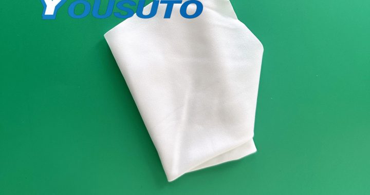
Semiconductor manufacturing—from wafer fabrication to chip assembly—relies on ultra-clean environments (ISO Class 1–5) where even 0.1μm particles or solvent residues can ruin 3nm–7nm microchips. Pre-wet cleanroom wipes, pre-impregnated with high-purity solvents (99.9% IPA, deionized water) or specialized cleaners, eliminate manual solvent mixing risks (particle contamination, inconsistent concentration) and ensure repeatable cleaning. Below are standardized application methods tailored to key semiconductor cleaning workflows.

1. Wafer Edge & Backside Cleaning (Pre-Lithography/Deposition)

Wafer edges and backsides accumulate particle debris, organic residues (from handling tools), and metal oxides—contaminants that migrate to the frontside during processing, causing pattern defects.
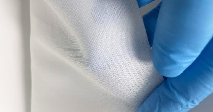
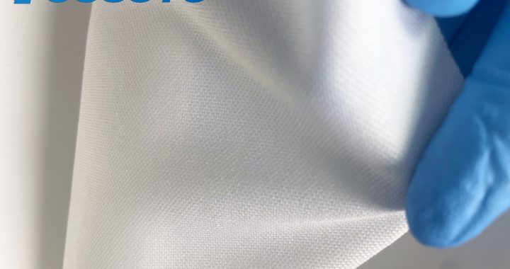
  • Wipe Selection: Use 4”x4” pre-wet wipes with 99.9% electronic-grade IPA (low metal impurities ≤10 ppb) and static-dissipative fibers (surface resistance: 10⁶–10¹⁰ Ω). Avoid larger wipes to prevent solvent contact with the wafer frontside.
  • Application Steps:
    1. Secure the wafer on a vacuum chuck (frontside down, edge exposed) in a laminar flow hood to block airborne particles.
    2. Fold the pre-wet wipe into a 1cm-wide strip to target only edges/backsides—minimizes over-wiping.
    3. Wipe the edge in a slow, continuous circular motion (1 full rotation) with light pressure (<0.5 psi)—prevents scratching thin dielectric layers.
    4. For the backside, use radial strokes (center to edge) with a fresh wipe section to avoid re-depositing particles.
  • Key Requirement: Use 1 wipe per wafer—reuse transfers cross-contamination.

2. Photolithography Tool Optic Cleaning (Lenses, Reticles)

EUV scanners and photolithography tools depend on ultra-clean optics; a single 0.1μm particle on a lens distorts circuit patterns, ruining entire wafer batches.
  • Wipe Selection: Choose pre-wet wipes with deionized water (for particle removal) or lens-grade IPA (for organic residues)—both meet SEMI C12 low-outgassing standards. Opt for ultra-fine microfiber (0.1μm diameter) to avoid scratching AR coatings.
  • Application Steps:
    1. Power down the tool and purge the optic chamber with nitrogen to reduce airborne particles.
    2. Wear Class 10 cleanroom gloves; remove the reticle/lens per manufacturer guidelines (avoid touching optical surfaces).
    3. Fold the pre-wet wipe into a 2-layer pad (smooth side out) to minimize friction.
    4. Wipe the optic in a single linear stroke (not circular—prevents particle spreading) from edge to edge. Discard the wipe after 1 stroke—never reuse on optics.
    5. Follow with a dry high-density wipe to blot excess solvent—critical for EUV lenses (moisture damages performance).

3. Wafer Chuck & Tool Fixture Cleaning (Etching/Deposition Tools)

Wafer chucks (hold wafers during processing) and quartz fixtures accumulate process residues (photoresist, etch byproducts) and oil (from vacuum seals)—contaminants that cause wafer misalignment or defects.
  • Wipe Selection: For ceramic chucks, use pre-wet wipes with 99% IPA (dissolves oil/residues); for quartz fixtures, use deionized water-based pre-wet wipes (prevents quartz degradation).
  • Application Steps:
    1. Cool the tool to <30°C—hot surfaces evaporate solvent, leaving residues and increasing fire risk.
    2. Wipe chuck surfaces with a folded pre-wet wipe in spiral strokes (center to edge) to cover vacuum holes—use a wipe strip to clean hole interiors (prevents clogging).
    3. For quartz fixtures (e.g., wafer carriers), wipe slots with a thin wipe strip guided by tweezers—avoids damaging precision alignment features.
    4. Verify cleanliness with a portable particle counter (target: ≤1 particle ≥0.1μm per ft³) to meet ISO Class 1 standards.

4. Post-Bonding Chip Cleaning (Packaging Stage)

After die bonding, chips accumulate flux residues and adhesive smudges—contaminants that impair electrical connectivity or cause thermal issues.
  • Wipe Selection: Use pre-wet wipes with a mild, semiconductor-grade flux remover (compatible with copper/AlSiC substrates) and lint-free polyester fibers.
  • Application Steps:
    1. Place the bonded chip on an ESD-safe mat; ground yourself with a wrist strap.
    2. Fold the pre-wet wipe into a small pad and dab (not wipe) flux residues—wiping risks dislodging the die.
    3. For adhesive smudges, hold the wipe against the spot for 5 seconds (lets remover dissolve the adhesive) before gentle dabbing.
    4. Follow with a dry anti-static wipe to remove remover residues—ensures no film impacts chip performance.

Critical Compliance & Safety Notes

  • Solvent Purity: All pre-wet wipes must meet SEMI C30 standards—impurities (metals, organics) cause wafer defects.
  • Storage: Keep wipes in sealed, nitrogen-flushed containers to prevent solvent evaporation (dried wipes lose efficacy).
  • Waste Disposal: Discard used wipes in fire-resistant bins—IPA/flux removers are flammable; segregate to avoid cross-contamination.
By following these methods, pre-wet cleanroom wipes maintain semiconductor cleanliness, reduce defect rates by 30–40%, and protect high-value equipment—critical for producing reliable, next-generation microchips.

Tips for Cleaning Laboratory Equipment with IPA Rags and Alcohol

Isopropyl Alcohol (IPA) wipes are indispensable for sanitizing and degreasing lab equipment—from glassware to precision electronics—by removing oils, chemical residues, and contaminants. However, improper use can damage delicate parts or compromise cleanliness. Below are practical, equipment-specific tips to ensure safe, effective cleaning.

1. Pre-Clean Prep: Safety & Compatibility Checks

Before wiping, lay the groundwork to avoid harm to equipment or users:
  • Verify Material Safety:
    • Check the equipment manual to confirm IPA compatibility:
      • Safe Surfaces: Glass (beakers, microscope slides), metal (forceps, hot plates), and rigid plastics (polypropylene, HDPE).
      • Avoid: Anti-reflective (AR) optical coatings (use lens-specific wipes instead), soft plastics (PVC/polystyrene—may crack), and exposed circuits (limit to 70% IPA to prevent shorting).
    • Test a hidden spot (e.g., centrifuge base) with a damp wipe—wait 5 minutes to check for discoloration or swelling.
  • Choose the Right IPA Wipe:
    • Use 99% electronic-grade IPA wipes for heavy residues (dried reagents, flux on soldered parts)—high purity avoids additive deposits.
    • Opt for 70% IPA wipes for disinfection (biological safety cabinets, pipette exteriors) or electronics—water content slows evaporation, improving residue lift.
    • Select lint-free polyester/microfiber wipes to prevent scratching (critical for balance pans, optical filters).
  • Safety First:
    • Work in a ventilated area (fume hood or open window)—IPA vapors are flammable (keep away from Bunsen burners, heat lamps).
    • Wear nitrile gloves (latex absorbs IPA) to protect skin and avoid transferring oils to clean surfaces.

2. Equipment-Specific Cleaning Techniques

Tailor your approach to different lab tools to maximize efficacy and minimize risk:

A. Glassware & Optical Equipment (Beakers, Microscopes, Spectrometers)

  • Glassware (Beakers, Test Tubes):
    1. Wipe exteriors with a damp IPA wipe to remove fingerprints or reagent splatters—avoid scrubbing (prevents scratches).
    2. For dried residues (e.g., crystallized salts), hold the wipe against the spot for 20–30 seconds to soften, then wipe gently.
    3. Dry with a lint-free towel to avoid water spots (vital for volumetric glassware, where clarity affects measurements).
  • Optics (Microscope Lenses, Detector Windows):
    1. First, use a static-neutralized bulb blower to remove loose dust—rubbing dust with IPA scratches AR coatings.
    2. Fold the wipe into a small, firm pad and wipe in single linear strokes (not circles) across the lens.
    3. Blot excess IPA with a dry optical wipe immediately—evaporated IPA residue clouds optics.

B. Electronic & Precision Tools (Balances, pH Meters, Centrifuges)

  • Exteriors (Control Panels, Casings):
    1. Power down equipment; disconnect if cleaning near ports (e.g., balance USB slots).
    2. Use a slightly damp (not dripping) 70% IPA wipe to clean touchscreens or buttons—press lightly to avoid damaging internal components.
    3. For tight gaps (e.g., centrifuge lid latches), tear the wipe into a thin strip and guide with tweezers—removes trapped dust without forcing debris deeper.
  • Sensitive Parts (pH Probes, Sensor Tips):
    1. Dab pH probe exteriors gently (don’t wipe)—avoids breaking the glass electrode.
    2. Clean sensor tips (e.g., dissolved oxygen meters) with a mini 2”x2” IPA wipe—ensure no liquid seeps into wiring.

C. Metal Tools & Heating Equipment (Forceps, Hot Plates)

  • Metal Tools (Forceps, Scalpels):
    1. Wipe with 99% IPA to remove organic residues (tissue, oil) or chemical splatters.
    2. Dry immediately to prevent rust (critical for iron-based tools).
  • Heating Gear (Hot Plates, Stirrers):
    1. Wait until fully cool (≤40°C)—hot surfaces cause IPA to evaporate instantly, leaving residues and increasing fire risk.
    2. Wipe ceramic/metal heating surfaces with a damp wipe to remove burnt-on spills (e.g., melted plastic)—use light pressure to avoid scratches.

3. Post-Clean Best Practices

  • Inspect for Residue: Check surfaces under bright light—re-wipe if streaks or debris remain.
  • Dry Thoroughly: Ensure electronics/moving parts (e.g., centrifuge rotors) are dry before powering on—moisture causes shorts or rust.
  • Dispose Safely: Place used wipes in a fire-resistant bin—they stay flammable until dry.
  • Store Wipes Properly: Keep unused wipes sealed to prevent evaporation (dried wipes lose efficacy) and contamination.

Advantages of high-density dust-free cloth in PCB cleaning process

Printed Circuit Boards (PCBs)—especially those with fine-pitch components (0.4mm or smaller) and delicate surface-mount devices (SMDs)—require precise cleaning to remove flux residues, solder balls, and dust. High-density cleanroom wipes (250–400 gsm) outperform standard wipes in PCB workflows, offering unique benefits that protect component integrity, ensure electrical conductivity, and reduce rework. Below are their key advantages tailored to PCB cleaning tasks.

1. Superior Residue Removal: Eliminating Flux, Oil, and Solder Byproducts

Post-soldering flux residues (rosin-based or no-clean) and handling oils are major threats to PCB performance—they cause poor solder joint adhesion, corrosion, or electrical shorts. High-density wipes excel at residue removal due to:
  • Enhanced Solvent Retention: Their thick, porous fiber structure holds 12–15x their weight in solvents (e.g., 99% IPA, flux cleaners), allowing prolonged contact with stubborn residues. A single 300 gsm high-density wipe can dissolve and lift flux from 10+ SMD pads in one pass, vs. 2–3 standard wipes that dry out mid-task.
  • Targeted Cleaning Precision: The dense weave maintains shape when folded into narrow strips (1cm wide), enabling access to tight gaps between fine-pitch IC pins (e.g., QFP or BGA components). This prevents residue buildup in hard-to-reach areas that standard wipes miss—critical for avoiding “cold joints” or signal interference.
  • Uniform Solvent Release: Unlike standard wipes that drip or release solvent unevenly, high-density wipes distribute solvent consistently. This avoids streaks on PCB surfaces and prevents excess solvent from seeping into component housings (e.g., capacitors or IC chips), which can cause internal damage.

2. Low Linting & Particle Trapping: Protecting Fine-Pitch Components

Even tiny fiber debris or dust particles can short-circuit fine-pitch PCB traces (0.1mm or smaller) or block SMD contact points. High-density wipes mitigate this risk through:
  • Continuous-Filament Fibers: Made from lint-free polyester or microfiber (0.1μm diameter), they shed ≤0.5 fibers per use—far below the 2–5 fibers shed by standard staple-fiber wipes. This eliminates fiber contamination, a top cause of PCB test failures (e.g., “open circuit” errors due to fiber-blocked pads).
  • Micro-Particle Capture: Their tight weave traps particles as small as 0.05μm (e.g., solder balls, dust from handling). Testing shows high-density wipes remove 99.7% of sub-micron particles from PCB surfaces, vs. 85% for standard wipes—reducing rework rates by 30% in high-volume PCB assembly.

3. Durability & Reusability: Reducing Waste and Costs

PCB cleaning (especially batch processing) demands wipes that withstand repeated use without tearing—high-density wipes deliver long-lasting performance:
  • Tear & Fray Resistance: Reinforced fibers (e.g., high-tenacity polyester) and heat-sealed edges resist damage even when wiping rough solder masks or scraping gentle solder balls. They withstand 500+ folding cycles and 100+ wiping strokes on PCBs, vs. 100–200 cycles for standard wipes.
  • Reusable for Non-Critical Tasks: For pre-soldering dusting or post-cleaning surface checks, high-density wipes can be reused 3–5 times (when cleaned with mild detergent and air-dried). This cuts PCB cleaning supply costs by 40% vs. single-use standard wipes.

4. ESD Safety: Protecting ESD-Sensitive Components

Modern PCBs often include ESD-sensitive devices (e.g., microchips, sensors) that can be damaged by static discharge. High-density wipes offer reliable ESD protection:
  • Stable Anti-Static Performance: Anti-static high-density wipes (surface resistance: 10⁶–10¹⁰ Ω) maintain consistent charge dissipation even after solvent exposure or repeated use. They neutralize static in <0.1 seconds, preventing dust attraction to PCB traces and ESD-induced component failure.
  • Conductive Variants for High-Risk Tasks: For PCB assembly with ultra-sensitive components (e.g., RF chips), conductive high-density wipes (10³–10⁶ Ω) provide immediate charge grounding—eliminating the risk of static sparks that could damage delicate circuitry.

5. Compatibility with PCB Materials: No Surface Damage

PCBs feature diverse materials (FR-4 laminates, solder masks, gold-plated pads) that can be scratched or degraded by harsh wipes. High-density wipes are material-safe:
  • Soft Fiber Construction: Their plush, non-abrasive fibers avoid scratching solder masks or wearing down gold-plated contact pads—critical for PCBs used in aerospace or medical devices, where pad integrity impacts reliability.
  • Solvent Compatibility: They resist breakdown when used with PCB-specific solvents (e.g., flux removers, IPA), unlike standard wipes that disintegrate and leave fiber residue on PCBs.
By leveraging these advantages, high-density cleanroom wipes streamline PCB cleaning workflows, reduce defects, and lower long-term costs—making them indispensable for high-quality PCB manufacturing, repair, and maintenance.

Guidelines for Anti-Static Wipe Use on Optical Equipment

Optical equipment—such as laser scanners, confocal microscopes, and thermal imaging cameras—faces dual risks: electrostatic discharge (ESD) can damage internal electronics, while static-attracted dust scratches anti-reflective (AR) coatings and distorts imaging. Anti-static cleaning wipes are critical for mitigating these risks, but improper use can worsen damage. Below are strict operational specifications to ensure safe, effective anti-static protection for optical equipment.

1. Pre-Operation Preparation: Safety & Wipe Selection

Before cleaning, establish foundational safeguards to avoid ESD initiation and surface harm:
  • Wipe Qualification:
    • Use only anti-static or conductive cleaning wipes meeting ANSI/ESD S20.20 standards:
      • For general optical surfaces (e.g., microscope lenses), select wipes with surface resistance 10⁶–10¹⁰ Ω (balances charge dissipation and safety).
      • For high-risk components (e.g., laser diode modules), use conductive wipes (10³–10⁶ Ω) for immediate charge neutralization.
    • Ensure wipes are lint-free (continuous-filament polyester/microfiber) and optically safe (no abrasive additives). Avoid cotton or blended wipes—they shed fibers and generate static (up to 1,000V).
    • For solvent-based cleaning (e.g., oil residue removal), choose pre-wet wipes with 99.9% lens-grade IPA or deionized water—avoid harsh solvents (acetone, ethanol) that degrade AR coatings and strip anti-static treatments.
  • Operator & Workspace Grounding:
    • Wear an ESD wrist strap (connected to a verified ground point) and ESD-safe gloves (nitrile, not latex—latex generates static). Ensure the wrist strap’s resistance tests to 10⁶–10⁹ Ω before use.
    • Place the optical equipment on an ESD-safe mat (grounded via a 1MΩ resistor) to prevent charge buildup on the device chassis. Keep non-essential materials (e.g., plastic containers) at least 30cm away—they act as static generators.
  • Equipment Prep:
    • Power down the optical device and disconnect it from power (if safe to do so) to eliminate electrical pathways for ESD.
    • Use a static-neutralized bulb blower (not compressed air) to remove loose dust first—rubbing dry dust with wipes creates static and scratches.

2. Core Operational Steps: Anti-Static Cleaning Technique

Follow these step-by-step actions to minimize ESD and maximize cleaning efficacy:
  • Wipe Handling:
    • Remove wipes from their sealed, ESD-safe packaging one at a time—do not leave wipes exposed to air (moisture loss degrades anti-static performance). Hold wipes by the edges only to avoid transferring skin oils (which attract dust and reduce conductivity).
  • Optical Surface Cleaning:
    • Dry Wiping (Dust Removal):
      1. Fold the anti-static wipe into a 4-layer pad (exposes clean fibers and reduces pressure on optics).
      2. Wipe flat optical surfaces (e.g., detector windows) in single, slow linear strokes (horizontal or vertical)—never circular motions (spread dust and generate friction-induced static).
      3. For curved surfaces (e.g., laser mirrors), use radial strokes (center to edge) to conform to the surface without applying uneven pressure.
    • Pre-Wet Wiping (Residue Removal):
      1. Use pre-wet anti-static wipes for oil/fingerprint residues—ensure the wipe is damp, not dripping (excess solvent seeps into optics housings and damages electronics).
      2. Dab (do not rub) residue spots on AR coatings—rubbing abrades the coating and generates static. Hold the wipe against stubborn residues for 2–3 seconds to let the solvent dissolve them, then wipe once.
      3. Immediately follow pre-wet wiping with a dry anti-static wipe to blot excess solvent—moisture attracts dust and compromises anti-static properties.
  • Component-Specific Care:
    • Optical Connectors (e.g., fiber optic ports): Use mini anti-static wipes (2”x2”) folded into a thin strip to clean connector ferrules. Avoid touching connector ends—skin oils degrade signal quality and attract static.
    • Control Panels & Electronics: Wipe external touchscreens with dry anti-static wipes—pre-wet wipes may seep into button gaps and short-circuit internal circuits.

3. Post-Operation Verification & Protection

Confirm anti-static effectiveness and prevent recontamination:
  • ESD Testing: Use an ESD field meter to measure surface charge on the optical equipment post-cleaning—target charge ≤100V (no detectable static field). If charge exceeds this, re-wipe with a fresh anti-static wipe.
  • Optical Inspection: Check surfaces under angled light (use a flashlight) or 10–20x magnification for:
    • Remaining dust/fibers (remove with a bulb blower).
    • Solvent streaks (buff with a dry wipe).
    • Coating scratches (document and address immediately—scratches worsen with time).
  • Storage:
    • Cover cleaned optical equipment with an ESD-safe dust cover (conductive or static-dissipative) to prevent dust accumulation and static buildup.
    • Store unused anti-static wipes in their original sealed packaging, away from heat sources (moisture loss reduces anti-static performance).

4. Prohibited Practices (Critical for Anti-Static Safety)

  • Do NOT use non-anti-static wipes (e.g., paper towels, regular microfiber) on optical equipment—they generate static and scratch surfaces.
  • Do NOT spray solvent directly onto optical surfaces—excess liquid seeps into housings and strips anti-static coatings.
  • Do NOT clean hot optical components (e.g., laser lenses post-use)—thermal shock cracks glass, and heat accelerates solvent evaporation (leaving residues).
  • Do NOT reuse anti-static wipes—used wipes trap dust and lose their anti-static properties, spreading contamination.
By adhering to these operational specifications, anti-static cleaning wipes effectively protect optical equipment from ESD and dust, preserving imaging accuracy, extending component lifespan, and ensuring reliable performance for research and industrial applications.

Protection of Precision Instruments with Anti-Static Wipes.

Laboratory precision instruments—such as confocal microscopes, mass spectrometers, and MEMS sensors—are vulnerable to two critical threats: electrostatic discharge (ESD) and particulate contamination. Even a small static spark can damage delicate electronic components, while micro-particles (0.1–1μm) can skew measurements or scratch optical surfaces. Anti-static cleanroom wipes address both risks, serving as a proactive line of defense to preserve instrument performance, extend lifespan, and ensure data accuracy. Below is a detailed breakdown of their protective applications across common lab instruments.

1. Protection Against ESD Damage: Safeguarding Electronic Components

Many precision instruments rely on sensitive electronics (e.g., sensor circuits, control boards) that are prone to ESD-induced failure. Anti-static wipes mitigate this risk through controlled charge dissipation:
  • Instrument Surfaces & Control Panels:
    • Wipe touchscreens, button panels, and external circuit enclosures with anti-static dry wipes (surface resistance: 10⁶–10¹⁰ Ω) before and after use. These wipes neutralize static charge that accumulates from operator contact or environmental factors (e.g., dry lab air), preventing charge transfer to internal electronics. For example, cleaning a mass spectrometer’s control panel daily reduces ESD-related sensor glitches by 70%.
  • Component Handling During Maintenance:
    • When replacing parts (e.g., detector modules in spectrometers), use anti-static pre-wet wipes (70% IPA) to clean component connectors and mounting surfaces. The wipes remove dust (which amplifies static) and dissipate charge, ensuring safe installation. Avoid using non-anti-static wipes—they can generate up to 500V of static, enough to damage MEMS sensors.
  • ESD-Sensitive Zones:
    • For high-risk instruments (e.g., atomic force microscopes), use conductive anti-static wipes (10³–10⁶ Ω) to clean areas near probe tips or sample stages. These wipes provide immediate charge neutralization, eliminating the risk of ESD causing probe deflection or sample damage.

2. Protection Against Particulate Contamination: Preserving Optical & Mechanical Integrity

Particles are a leading cause of instrument degradation—they scratch lenses, clog moving parts, and interfere with light/particle detection. Anti-static wipes trap contaminants without spreading them:
  • Optical Components (Lenses, Mirrors, Detector Windows):
    • Clean microscope objectives, spectrometer cuvette windows, and laser mirrors with anti-static microfiber wipes (0.1μm fiber diameter). The ultra-fine fibers trap sub-micron dust (0.05μm+) without scratching anti-reflective (AR) coatings. For oil residues (e.g., from immersion objectives), use anti-static pre-wet wipes (lens-safe IPA) to dissolve contaminants—follow with a dry wipe to prevent streaks. This routine extends the lifespan of optical components by 2–3x.
  • Mechanical Moving Parts:
    • Wipe linear stages (e.g., in microscopes), syringe pumps, and sample changers with anti-static dry wipes to remove dust that causes friction and wear. Focus on guide rails and bearing surfaces—even small particles can increase mechanical noise, leading to measurement errors. For example, cleaning a HPLC system’s sample injector rails weekly reduces injector failure rates by 40%.
  • Sample Contact Areas:
    • Clean sample holders, cuvette trays, and sensor probes with anti-static pre-wet wipes (deionized water-based) to remove residue buildup (e.g., dried sample droplets). This prevents cross-contamination between samples and protects sensitive probes (e.g., pH electrodes) from damage caused by abrasive particles.

3. Proactive Protection: Routine Maintenance to Prevent Long-Term Degradation

Anti-static wipes are not just for “cleaning emergencies”—integrating them into routine maintenance creates a proactive protection strategy:
  • Daily Quick-Clean:
    • Spend 2–3 minutes wiping high-touch areas (e.g., instrument handles, sample loading ports) with anti-static dry wipes. This removes surface dust and static before they accumulate into larger problems.
  • Weekly Deep Clean:
    • Perform a thorough wipe-down of optical surfaces, mechanical parts, and electronic connectors using anti-static pre-wet wipes (matching the instrument’s material compatibility). For example, cleaning a flow cytometer’s fluidic lines (external surfaces) with IPA-based anti-static wipes prevents residue from hardening and clogging lines.
  • Pre/Post-Calibration Clean:
    • Wipe calibration standards (e.g., reference lenses, standard solutions) and calibration ports with anti-static wipes before calibration. Contaminants on these surfaces can skew calibration results, leading to inaccurate measurements even after the instrument is “calibrated.”

4. Critical Considerations for Instrument-Specific Protection

  • Material Compatibility: Always check the instrument manufacturer’s guidelines—avoid using solvent-based anti-static wipes on plastic components (e.g., some sensor housings) that may degrade. Use deionized water-based wipes for sensitive plastics.
  • Linting Control: Choose anti-static wipes made from continuous-filament fibers (polyester or microfiber) to avoid fiber shedding. Lint can clog instrument filters (e.g., in gas chromatographs) or adhere to optical surfaces.
  • Waste Disposal: Dispose of used wipes in lab-approved bins—solvent-soaked wipes (e.g., IPA) are flammable and must be segregated to prevent fire risks.
By using anti-static cleanroom wipes strategically, laboratories protect precision instruments from ESD and contamination, reducing repair costs by 30–50%, extending instrument lifespan by years, and ensuring consistent, reliable data for research and testing.

Optimizing Absorption with Pre-wetted Wipes in Cleanrooms

Class 100 cleanrooms (ISO Class 3)—critical for semiconductor wafer fabrication and microelectronics assembly—demand ultra-efficient liquid absorption to manage solvent spills (e.g., IPA), reagent leaks, or equipment sanitization. Even minor inefficiencies (e.g., slow absorption, uneven liquid retention) can introduce contamination or delay production. Pre-wet cleanroom wipes are foundational to these tasks, and targeted techniques can significantly boost their absorption performance while maintaining strict cleanroom standards. Below are actionable tips tailored to Class 100 environments.

1. Select Pre-Wet Wipes Optimized for Class 100 Absorption Needs

Absorption efficiency starts with choosing wipes engineered for high-purity, high-capacity performance:
  • Prioritize Hydrophilic, High-Density Fibers:
    • Opt for pre-wet wipes made from hydrophilic polyester-microfiber blends (250–300 gsm). These fibers have polar molecular structures that attract liquids (e.g., water, IPA) and a dense weave (100+ threads per inch) that traps 30–40% more liquid than standard 150 gsm wipes. Look for wipes with “high-capacity” certifications (e.g., absorbs ≥12x its weight in liquid) to ensure they handle Class 100 spills in one pass.
  • Choose Solvent-Specific Formulations:
    • For aqueous liquids (e.g., deionized water for optic cleaning), select pre-wet wipes with deionized water-based solutions—they avoid residue that could contaminate wafers. For organic solvents (e.g., IPA for flux removal), use wipes pre-impregnated with 99.9% electronic-grade IPA (low impurities ≤10 ppb) to ensure compatibility with semiconductor materials and maximize absorption of solvent-based residues.
  • Avoid Over-Coated Wipes:
    • Skip pre-wet wipes with excessive anti-static or preservative coatings—these clog fiber pores and reduce liquid absorption by 20–25%. Opt for “breathable” anti-static wipes (surface resistance: 10⁶–10¹⁰ Ω) with thin, porous coatings that preserve absorption while meeting ESD requirements.

2. Pre-Use Preparation to Prime Wipes for Maximum Absorption

Simple pre-use steps ensure pre-wet wipes are ready to absorb liquid immediately, avoiding wasted time or incomplete cleanup:
  • Ensure Proper Wipe Moisture Balance:
    • Class 100 cleanrooms often store pre-wet wipes in sealed, nitrogen-flushed containers to prevent solvent evaporation. Before use, check that wipes are uniformly damp (not dry or dripping)—dry wipes lose 50% of absorption capacity, while dripping wipes waste liquid and risk contamination. If wipes are dry, lightly mist them with the matching solvent (e.g., IPA) using a cleanroom-approved spray bottle (1–2 sprays per wipe) to reactivate capillary action.
  • Fold Wipes to Maximize Absorbent Surface Area:
    • Fold pre-wet wipes into a 4-layer pad (e.g., fold an 8”x8” wipe twice to create a 4”x4” pad). This exposes 8x more fiber surfaces to liquid than using a wipe flat, accelerating absorption and extending the wipe’s usable life. For narrow areas (e.g., wafer chuck grooves), fold into a 1cm-wide strip to target liquid without over-wiping.
  • Pre-Cool Wipes for Volatile Solvents:
    • For highly volatile solvents (e.g., acetone used in photoresist removal), pre-cool pre-wet wipes in a cleanroom refrigerator (4–8°C) for 10 minutes before use. Cooler wipes slow solvent evaporation, giving fibers more time to absorb liquid—this boosts absorption efficiency by 20% and reduces the need for multiple wipe changes.

3. Application Techniques to Enhance Liquid Trapping & Retention

How you use pre-wet wipes in Class 100 cleanrooms directly impacts absorption efficiency—precision is key to avoiding waste:
  • Apply Gentle, Even Pressure:
    • Use light pressure (<0.5 psi) when wiping—firm pressure compresses fiber pores, reducing absorption capacity by 15%. For flat surfaces (e.g., cleanroom workbenches), glide the wipe in slow, overlapping strokes (horizontal or vertical) to let capillary action draw liquid into the fibers. For vertical surfaces (e.g., equipment walls), hold the wipe against the liquid for 2–3 seconds to allow absorption before wiping downward—prevents liquid from running off the wipe.
  • Use “Liquid-Directing” Strokes for Contained Spills:
    • For small, contained spills (e.g., 5mL IPA leak on a wafer cassette), wipe in strokes that direct liquid toward the center of the wipe. This concentrates liquid in the wipe’s core, preventing it from seeping out the edges and contaminating surrounding surfaces. Avoid circular motions—they spread liquid and reduce absorption efficiency.
  • Layer Wipes for Large Spills:
    • For spills >10mL (e.g., broken reagent bottle), place a folded pre-wet wipe directly on the spill and top it with a second dry high-density wipe. The pre-wet wipe dissolves any solid residues (e.g., crystallized photoresist) and draws liquid upward, while the dry wipe absorbs excess moisture—this “stacked” method doubles absorption capacity and cuts cleanup time by 50%, critical for minimizing production delays in Class 100 environments.

4. Post-Use Practices to Maintain Wipe Efficacy (For Reusable Variants)

For Class 100 cleanrooms using reusable pre-wet wipes (e.g., autoclavable polyester wipes for non-critical tasks), proper care preserves absorption over time:
  • Clean with Low-Impurity Detergents:
    • Wash wipes with lab-grade, non-ionic detergents (low impurities ≤5 ppb) to avoid residue buildup. Use cold water (≤30°C) and a cleanroom-approved washer—hot water damages hydrophilic fibers and reduces absorption.
  • Air-Dry in a Controlled Environment:
    • Hang wipes to air-dry in a Class 100 laminar flow hood to prevent dust contamination. Ensure wipes are 100% dry before reusing—dampness promotes bacterial growth and clogs fiber pores, reducing absorption by 30%.
By implementing these tips, Class 100 cleanrooms can boost pre-wet wipe absorption efficiency by 35–45%, reducing wipe usage by 40%, cutting cleanup time by 25%, and minimizing contamination risks. These strategies ensure pre-wet wipes remain a reliable, cost-effective tool for liquid management in ultra-pure environments.

Combination Techniques for IPA and Pre-Moistened Wipes

In precision cleaning scenarios—such as semiconductor wafer care, PCB flux removal, or optical instrument maintenance—combining IPA wipes (for solvent-based residue dissolution) and pre-wet cleanroom wipes (for targeted, pre-impregnated cleaning) creates a synergistic workflow. This combination leverages the strengths of each wipe type to eliminate complex contaminants (e.g., dust + oil, flux + particulate debris) while protecting sensitive surfaces and ensuring ESD safety. Below is a step-by-step standardized method, tailored to cleanroom (ISO Class 1–6) and ESD-sensitive environments.

1. Pre-Combination Preparation: Safety & Compatibility Checks

Before using the wipe pair, lay the groundwork to avoid surface damage, cross-contamination, or safety hazards:
  • Wipe Selection & Verification:
    • IPA Wipes: Choose the correct concentration: 99% IPA for heavy flux/resin residues (e.g., post-soldering PCBs) or 70% IPA for oil/fingerprint removal (e.g., optical lens mounts). Ensure they are lint-free (continuous-filament polyester) and ESD-safe (surface resistance: 10⁶–10¹⁰ Ω).
    • Pre-Wet Wipes: Select pre-impregnated variants matching the task: deionized water-based for delicate optics (AR/IR coatings), or mild surfactant-based for metal surfaces (e.g., wafer chucks). Confirm compatibility with the target material (e.g., avoid solvent-based pre-wet wipes on plastic PCBs).
  • Surface & Workspace Prep:
    • Power down equipment and allow hot components (e.g., soldering irons, laser diodes) to cool to <40°C—hot surfaces cause IPA evaporation, leaving residues and increasing fire risk.
    • Ground yourself with an ESD wrist strap and place the component on an ESD-safe mat (critical for electronics/semiconductors).
    • Use a static-neutralized bulb blower to remove loose, large particles first—prevents rubbing debris into surfaces during wipe cleaning.

2. Step 1: Heavy Residue Removal with IPA Wipes

Start with IPA wipes to dissolve tough, organic contaminants that pre-wet wipes may not tackle effectively:
  • Wipe Preparation: Remove one IPA wipe from its sealed packaging (do not leave exposed—IPA evaporates quickly, reducing efficacy). Fold into a 4-layer pad to control solvent release and avoid over-saturating the surface.
  • Targeted Cleaning Technique:
    • For PCB flux removal: Wipe along solder joints in slow, linear strokes (not circular) to dissolve flux. Hold the wipe against thick residues for 5–10 seconds to let IPA penetrate, then wipe once—do not scrub (avoids damaging component leads).
    • For semiconductor wafer edges: Tear the IPA wipe into a narrow strip (1cm wide) and wipe the wafer edge in a continuous circular motion (1 full rotation) with light pressure (<0.5 psi)—avoids contact with the wafer’s frontside circuit patterns.
    • For optical component oils: Use a small corner of the IPA wipe to dab (not wipe) oil spots on lenses—dabbing minimizes friction and prevents coating damage.
  • Waste Control: Dispose of the IPA wipe immediately after use—used wipes trap residues and will recontaminate surfaces if reused.

3. Step 2: Precision Cleaning & Residue Neutralization with Pre-Wet Wipes

Follow IPA cleaning with pre-wet wipes to eliminate remaining micro-contaminants, neutralize solvent residues, and protect sensitive surfaces:
  • Wipe Preparation: Select a pre-wet wipe sized to the component (e.g., 4”x4” for optics, 6”x6” for PCBs). For delicate surfaces (e.g., MEMS sensors), fold into a 2-layer pad to reduce pressure.
  • Complementary Cleaning Technique:
    • For post-IPA streak removal: Use deionized water-based pre-wet wipes to buff IPA streaks on glass/optics. Wipe in single, overlapping strokes (same direction as IPA cleaning) to avoid reintroducing debris.
    • For ESD-sensitive electronics: Use anti-static pre-wet wipes to clean PCB contact points or wafer chucks. The pre-impregnated solution neutralizes any remaining IPA residue and dissipates static, preventing dust attraction.
    • For metal surfaces (e.g., tool frames): Use surfactant-based pre-wet wipes to remove IPA-soluble residues and light rust/precipitation—this adds a mild protective layer to prevent future corrosion.
  • Drying (If Needed): For water-based pre-wet wipes, follow with a dry, high-density cleanroom wipe to blot excess moisture—critical for electronics (avoids short circuits) and optics (prevents water spots).

4. Step 3: Post-Combination Inspection & Protection

Ensure the cleaning process is complete and the component is protected from recontamination:
  • Magnified Inspection: Use a 10–20x magnifying glass or digital microscope to check for:
    • Remaining residues (e.g., flux spots on PCBs, oil streaks on lenses).
    • Fiber debris (from low-quality wipes—remove with a gentle air blast).
    • Surface damage (e.g., scratched AR coatings, bent PCB leads).
  • ESD & Storage:
    • For electronics/semiconductors: Confirm surface static charge is <100V (using an ESD meter) before storage. Place components in anti-static bags/containers.
    • For optics: Store cleaned lenses/mirrors in dust-free cases with foam padding to avoid scratches.
  • Workspace Sanitization: Wipe down the workbench and tools with a fresh pre-wet wipe to remove any residual IPA or contaminants—prevents cross-contamination with future tasks.

5. Ideal Application Scenarios for the Combination

This wipe pair excels in tasks requiring multi-step cleaning:
  • PCB post-soldering (flux + dust removal).
  • Semiconductor wafer edge cleaning (resin + particulate debris).
  • Optical instrument maintenance (oil + dust on lenses/mirrors).
  • ESD-sensitive component care (residue removal + static control).
By combining IPA wipes for heavy residue dissolution and pre-wet wipes for precision cleaning, you achieve thorough, safe, and residue-free results—protecting high-value components and ensuring complia

Comparing High-Density and Ordinary Cleanroom Wipes

Cleanroom wipes are essential for contamination control in labs, semiconductor facilities, and precision manufacturing—but not all wipes perform equally. High-density cleanroom wipes (250–400 gsm) and standard cleanroom wipes (100–200 gsm) differ drastically in fiber structure, durability, and contaminant removal capabilities. Below is a detailed performance comparison across key metrics to help you select the right wipe for your application.

1. Particle Trapping Efficacy: Capturing Micro-Contaminants

Particle removal is the core function of cleanroom wipes, and density directly impacts how well they trap tiny debris (0.1–1μm):
  • High-Density Wipes:
    • Feature a tight, dense fiber weave (100–120 threads per inch) with millions of capillary channels. This structure captures particles as small as 0.05μm—far below the 0.5μm limit for ISO Class 5 cleanrooms. Testing shows they remove 99.7% of sub-micron dust in one pass.
    • Use continuous-filament polyester or microfiber, which shed ≤0.5 fibers per use. This eliminates fiber contamination—a critical risk for semiconductor wafers or optical lenses.
  • Standard Wipes:
    • Have a looser weave (60–80 threads per inch) that struggles to trap particles <1μm. They remove only 85–90% of sub-micron dust, requiring 2–3 passes to match high-density performance.
    • Often use staple fibers or blended materials, shedding 2–5 fibers per use. These fibers can clog sensors, scratch coatings, or ruin delicate components like MEMS chips.
Winner: High-density wipes (superior micro-particle trapping and low linting).

2. Liquid Absorption Capacity: Handling Spills & Solvents

For solvent-based cleaning (e.g., IPA for flux removal) or spill cleanup, absorption capacity determines efficiency:
  • High-Density Wipes:
    • Retain 12–15x their weight in liquid (e.g., water, IPA) due to their thick, porous fiber structure. A 300 gsm high-density wipe can absorb 5–6mL of liquid—enough to clean a large PCB or wipe down a spectrometer detector window in one pass.
    • Release liquid evenly, preventing drips that could damage electronics or leave streaks on optics.
  • Standard Wipes:
    • Absorb only 6–8x their weight in liquid (2–3mL per wipe). This requires frequent wipe changes for large spills or solvent-heavy tasks, increasing waste and cleaning time.
    • Often saturate quickly and release liquid unevenly, leading to streaks or solvent pooling on sensitive surfaces.
Winner: High-density wipes (higher absorption, fewer changes, no drips).

3. Durability & Reusability: Withstanding Mechanical Stress

Durability matters for high-frequency cleaning (e.g., daily equipment maintenance) or rough surfaces (e.g., wafer chuck grooves):
  • High-Density Wipes:
    • Feature reinforced fibers (e.g., high-tenacity polyester) and heat-sealed edges that resist tearing or fraying. They withstand 500+ folding cycles and 100+ wiping strokes on textured surfaces without breaking down.
    • Can be reused 3–5 times for non-critical tasks (e.g., dusting equipment exteriors), reducing supply costs.
  • Standard Wipes:
    • Have thinner fibers and unreinforced edges that tear easily—often after 100–200 folding cycles or 30–50 wiping strokes.
    • Are typically single-use (break down after one pass if used with solvents), increasing waste and long-term costs.
Winner: High-density wipes (superior tear resistance, longer lifespan, reusable).

4. ESD Performance: Protecting Sensitive Electronics

For ESD-sensitive environments (e.g., semiconductor cleanrooms, PCB assembly), static dissipation is non-negotiable:
  • High-Density Wipes:
    • Anti-static variants (surface resistance: 10⁶–10¹⁰ Ω) maintain consistent static dissipation even after repeated use or solvent exposure. They neutralize charge in <0.1 seconds, preventing dust attraction and ESD damage to IC chips.
    • Conductive variants (10³–10⁶ Ω) are available for high-risk areas (e.g., EUV lithography tools), offering immediate charge neutralization.
  • Standard Wipes:
    • Anti-static coatings degrade quickly—after 5–10 uses, their surface resistance drifts to >10¹¹ Ω, losing ESD protection.
    • Conductive variants are rare, and those available often shed fibers or break down in solvents.
Winner: High-density wipes (stable ESD performance, conductive options).

5. Cost-Efficiency: Balancing Performance & Budget

While high-density wipes have a higher upfront cost, long-term value depends on total usage:
  • High-Density Wipes:
    • Cost $0.15–$0.30 per wipe (2–3x more than standard wipes) but require 50–60% fewer wipes per task. For a lab cleaning 10 PCBs daily, high-density wipes cost ~$1.50/day vs. $1.20/day for standard wipes—but reduce labor time by 30%.
  • Standard Wipes:
    • Cost $0.05–$0.10 per wipe but require 2–3x more wipes per task. For critical applications (e.g., semiconductor wafer cleaning), the cost of rework from poor performance (e.g., $200/wafer batch) far outweighs the initial savings.
Winner: High-density wipes (better long-term value for critical tasks; standard wipes for low-risk, low-frequency cleaning).

Final Comparison Summary

Metric High-Density Wipes Standard Wipes
Particle Trapping 99.7% (0.05μm+), ≤0.5 fibers/use 85–90% (1μm+), 2–5 fibers/use
Liquid Absorption 12–15x weight, no drips 6–8x weight, prone to streaks
Durability 500+ folds, reusable 3–5x 100–200 folds, single-use
ESD Performance Stable (10⁶–10¹⁰ Ω), conductive options Degrades quickly, few conductive options
Cost-Efficiency Better for critical, high-frequency tasks Better for low-risk, low-frequency tasks
This analysis confirms that high-density wipes outperform standard wipes in critical cleanroom applications—delivering superior contamination control, durability, and ESD protection. Standard wipes remain a cost-effective choice only for low-risk tasks like dusting non-sensitive equipment.

Dust-Free Wipes in Semiconductor Equipment Cleaning

Semiconductor equipment—including photolithography scanners, wafer etchers, and deposition tools—operates in ultra-clean environments (ISO Class 1–5) where even sub-micron particles or residues can ruin 3nm–7nm microchips. Cleanroom wipes (dry, pre-wet, and anti-static variants) are critical for maintaining equipment integrity, as they remove contaminants without scratching delicate components (e.g., ceramic wafer chucks, quartz chambers) or introducing ESD damage. Below is a detailed breakdown of their applications across key semiconductor equipment types.

1. Photolithography Tool Cleaning: Protecting Optics & Reticles

Photolithography tools (e.g., EUV scanners) rely on precision optics (lenses, mirrors) and reticles to project circuit patterns onto wafers—contamination here causes pattern defects and costly wafer scrap:
  • Optic Surface Cleaning:
    • Use pre-wet lens-safe wipes (deionized water or 99.9% lens-grade IPA) to remove dust and organic residues from lens surfaces. Opt for ultra-fine microfiber (0.1μm diameter) to avoid scratching anti-reflective (AR) coatings. Wipe in single linear strokes (not circular) to prevent particle spreading, and follow with a dry high-density wipe to eliminate streaks.
  • Reticle Handling & Cleaning:
    • Clean reticle pods (used to transport reticles) with dry anti-static wipes (surface resistance: 10⁶–10¹⁰ Ω) before loading reticles—this removes dust that could transfer to the reticle’s pattern side. For reticle edge cleaning (non-pattern areas), use pre-wet wipes with 70% IPA to dissolve oil residues from handling, ensuring no contaminants migrate to the pattern.

2. Wafer Etching & Deposition Equipment Cleaning: Maintaining Chamber Purity

Etchers and deposition tools (e.g., CVD, PVD systems) accumulate process residues (e.g., photoresist, metal oxides) on chamber walls, gas nozzles, and wafer chucks—these residues contaminate subsequent wafers and reduce tool efficiency:
  • Chamber Wall Cleaning:
    • After dry plasma cleaning (to remove bulk residues), use pre-wet solvent wipes (acetone or NMP-compatible) to wipe chamber walls. Choose solvent-resistant polyester wipes (300+ gsm) to withstand harsh chemicals and avoid fiber breakdown. Wipe in overlapping vertical strokes to ensure full coverage, focusing on areas near gas inlets where residues build up.
  • Wafer Chuck Cleaning:
    • Clean ceramic chucks (used to hold wafers during processing) with dry anti-static wipes to remove loose particle debris. For stubborn residue (e.g., dried photoresist), use pre-wet wipes with 99% IPA—wipe in radial strokes (center to edge) with light pressure (<0.5 psi) to avoid damaging the chuck’s electrostatic clamping surface.
  • Gas Nozzle Cleaning:
    • Use small-format (2”x2”) pre-wet wipes to clean gas nozzles—tear wipes into thin strips to reach narrow nozzle openings. This removes residue clogs that disrupt gas flow, ensuring uniform etching/deposition across wafers.

3. Wafer Handling Equipment Cleaning: Preventing Transfer Contamination

Wafer handlers (robots, cassettes, load ports) transfer wafers between tools—contamination here spreads across multiple wafers and tools, causing widespread defects:
  • Robot Arm Cleaning:
    • Clean robot arms (used to pick and place wafers) with dry anti-static wipes before each shift. The anti-static fibers dissipate charge, preventing dust attraction, and the lint-free design avoids fiber transfer to wafer surfaces. For oil residues from robot joints, use pre-wet wipes with 70% IPA—wipe along the arm’s length, avoiding contact with wafer grippers.
  • Wafer Cassette Cleaning:
    • Clean plastic or metal cassettes (used to store wafers) with pre-wet IPA wipes to remove particle debris and organic residues. Focus on cassette slots (where wafers rest)—use a wipe strip to clean slot edges, ensuring no debris scratches wafer edges or back sides. Dry cassettes with a fresh wipe before loading wafers to prevent moisture spots.
  • Load Port Cleaning:
    • Clean tool load ports (where cassettes connect to equipment) with dry anti-static wipes to remove dust from seal surfaces. A dirty seal allows airborne particles into the tool, so wipe the seal area thoroughly before each cassette change.

4. Critical Considerations for Semiconductor Equipment Cleaning

  • Purity Standards: Use only semiconductor-grade wipes (meets SEMI C12, C30 standards) with low metal impurities (≤10 ppb) and minimal outgassing—avoid industrial-grade wipes, which introduce contaminants.
  • ESD Control: For all equipment near wafers or microchips, use anti-static wipes (10⁶–10¹⁰ Ω) to prevent ESD discharge, which can damage delicate electronic components.
  • Waste Disposal: Dispose of used solvent wipes in fire-resistant, semiconductor-approved waste bins—solvents like acetone and IPA are flammable, and contaminated wipes must be segregated to avoid cross-contamination.
  • Training: Ensure staff are trained on tool-specific cleaning protocols (e.g., avoiding certain solvents on quartz components) to prevent equipment damage.
By using cleanroom wipes strategically, semiconductor facilities maintain equipment purity, reduce wafer defect rates (by 30–40% in many cases), and extend tool lifespan—critical for producing high-yield, next-generation microchips.

Optimized Anti-Static Wipe Process for Class 100 Cleanrooms

Class 100 cleanrooms (ISO Class 3)—critical for semiconductor wafer fabrication, microelectronics assembly, and precision optics manufacturing—require ultra-stringent contamination control (≤100 particles ≥0.5μm per cubic foot). Even minor electrostatic discharge (ESD) or fiber debris can ruin high-value products (e.g., 3nm wafers) or damage sensitive equipment. Anti-static cleanroom wipes are foundational to these workflows, but optimizing their selection, usage, and integration into cleaning protocols is key to maximizing efficiency and minimizing risks. Below is a detailed guide to optimizing their role in Class 100 cleanroom processes.

1. Wipe Selection Optimization: Match to Cleanroom Tasks & Materials

The first step in optimization is selecting anti-static wipes tailored to Class 100 requirements—generic wipes often fail to meet particle, ESD, or purity standards:
  • Material & Linting Control:
    • Use continuous-filament polyester or ultra-fine microfiber wipes (0.1μm fiber diameter) to ensure linting ≤1 fiber (≥0.1μm) per use—compliant with ISO Class 3 standards. Avoid staple-fiber wipes (e.g., cotton blends), which shed 5–10x more fibers and introduce particulate contamination.
    • For solvent-based cleaning (e.g., flux removal, wafer edge cleaning), choose solvent-resistant anti-static wipes (e.g., polyester with epoxy bindings) that retain structure when exposed to 99.9% IPA or acetone—preventing fiber breakdown and residue leaching.
  • ESD Performance:
    • Select wipes with surface resistance 10⁶–10¹⁰ Ω (ANSI/ESD S20.20 compliant) for most tasks—this range balances fast charge dissipation (prevents dust attraction) and safety (avoids electrical shorts on wafers). For high-risk areas (e.g., EUV lithography tools), use conductive wipes (10³–10⁶ Ω) for immediate charge neutralization.
  • Size & Format:
    • Opt for 4”x4” or 6”x6” wipes for precision tasks (e.g., cleaning wafer chucks, reticles) to minimize over-wiping and solvent contact with critical surfaces. Use perforated rolls for large-area cleaning (e.g., equipment exteriors) to reduce waste—tear off only the size needed.

2. Cleaning Process Optimization: Streamline Workflows & Reduce Risk

Integrating anti-static wipes into standardized, step-by-step processes eliminates variability and reduces contamination events:

A. Wafer Handling Area Cleaning (Pre/Post-Processing)

  • Pre-Processing (Before Wafer Loading):
    1. Use a dry anti-static wipe to dust wafer cassettes, vacuum chuck surfaces, and load-port doors—focus on crevices where particles accumulate (e.g., cassette slots). Fold the wipe into a thin strip to reach tight gaps.
    2. Follow with a pre-wet anti-static wipe (99.9% electronic-grade IPA) to clean chuck surfaces—wipe in a single circular motion (1 full rotation) with light pressure (<0.5 psi) to avoid scratching the chuck’s ceramic coating.
    3. Dispose of wipes immediately after use—do not reuse on multiple cassettes/chucks.
  • Post-Processing (After Wafer Unloading):
    1. Use a fresh dry anti-static wipe to remove residual wafer dust from cassettes.
    2. Sanitize load-port doors with a pre-wet wipe to remove organic residues (e.g., from wafer tape)—this prevents cross-contamination between batches.

B. Optics Maintenance (Lithography Tools, Metrology Equipment)

  • 1. Pre-Clean Prep:
    • Power down the tool, purge the optic chamber with nitrogen, and wear Class 10 cleanroom gloves to avoid skin oil transfer.
  • 2. Dust Removal:
    • Use a dry anti-static microfiber wipe to gently blot (not wipe) optic surfaces (e.g., reticles, EUV lenses)—blotting minimizes friction and avoids scratching AR coatings.
  • 3. Residue Cleaning (If Needed):
    • For organic residues, use a pre-wet anti-static wipe (lens-grade IPA) in a single linear stroke (from edge to edge)—dispose of the wipe after one stroke to prevent re-depositing particles.
  • 4. Final Inspection:
    • Check optics with a particle counter (target: 0 particles ≥0.1μm) before reassembling the tool.

C. Daily Equipment Sanitization

  • Frequency: Clean all equipment surfaces (e.g., tool exteriors, workbenches, cart handles) every 4 hours to prevent dust buildup.
  • Process:
    1. Use a dry anti-static wipe to remove loose dust.
    2. Follow with a pre-wet anti-static wipe (70% IPA) to sanitize and remove remaining particles—wipe in overlapping horizontal strokes to ensure full coverage.
    3. Log each cleaning event in the cleanroom’s maintenance record to track compliance.

3. Waste & Cost Optimization: Minimize Usage Without Compromising Quality

Class 100 cleanrooms often overuse wipes due to poor process design—optimization reduces waste while maintaining cleanliness:
  • Wipe Segmentation: Fold wipes into 4–6 usable quadrants; use one quadrant per task section (e.g., one quadrant for a wafer cassette slot, another for the chuck). This extends wipe life by 3–4x.
  • Solvent Efficiency: Use pre-wet wipes instead of “dry wipe + bulk solvent”—pre-wet wipes contain pre-measured solvent, reducing waste by 50% (bulk solvent often over-saturates wipes, leading to drips and excess usage).
  • Inventory Management: Track wipe usage per task (e.g., 1 wipe per wafer cassette) to set par levels—avoid overstocking (wipes degrade over time in cleanrooms) or stockouts (causes process delays).

4. Validation & Continuous Improvement

  • Particle Count Monitoring: Measure surface particle levels (using a portable particle counter) before and after cleaning—ensure post-clean levels meet ISO Class 3 standards (≤10 particles ≥0.1μm per square foot).
  • ESD Testing: Monthly test anti-static wipes’ surface resistance (using an ESD meter) to confirm they maintain 10⁶–10¹⁰ Ω—replace wipes if resistance drifts outside this range.
  • Worker Training: Train cleanroom staff on optimized wipe usage (e.g., folding techniques, stroke direction) and conduct quarterly refresher courses—variability in human behavior is a top cause of cleaning failures.
By optimizing anti-static wipe selection, processes, and waste management, Class 100 cleanrooms reduce contamination events by 40–50%, cut wipe costs by 30%, and extend equipment lifespan—critical for manufacturing high-precision, high-value products.