Pre-Wetted Wipes for Dust Removal from Precision Components

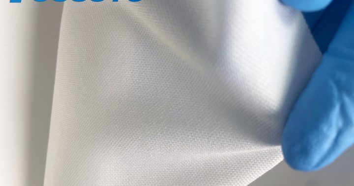
Precision components—such as microchips, sensor diaphragms, fiber optic connectors, and MEMS devices—have ultra-sensitive surfaces; even 0.1μm dust particles can cause functional failures, signal interference, or irreversible scratches. Pre-wet cleanroom wipes—pre-impregnated with low-residue solvents (deionized water, lens-grade IPA) or sterile cleaners—offer a gentle yet effective solution for dust removal, avoiding the risks of dry wiping (scratching) or compressed air (forcing dust into crevices). Below is a step-by-step method tailored to protect these delicate components.

1. Pre-Clean Preparation: Minimize Risk & Control Contamination

Proper prep is critical to prevent dust reattachment and component damage before wet cleaning:
  • Component & Workspace Prep:
    1. Ground the Workspace: Place the precision component on an ESD-safe mat and wear an ESD wrist strap (calibrated to 10⁶–10⁹ Ω) to eliminate static—static charges attract dust and can damage microelectronics.
    2. Reduce Airborne Dust: Clean the workbench with a lint-free dry wipe and use a laminar flow hood (if available) to create a particle-free zone. Turn off fans or air vents nearby to avoid stirring up dust during cleaning.
    3. Inspect the Component: Use a 20–40x magnifying glass to map dust locations (e.g., connector pins, sensor edges)—this ensures targeted cleaning and avoids unnecessary wipe contact with sensitive areas.
  • Pre-Wet Wipe Selection:
    1. Match Wipes to Component Type:
      • For electronics (microchips, PCBs): Choose pre-wet wipes with 70% lens-grade IPA (low conductivity, avoids short circuits) and ultra-fine microfiber (0.1μm diameter) to prevent scratching.
      • For optical components (fiber optic tips, lens arrays): Use deionized water-based pre-wet wipes—avoids solvent damage to anti-reflective (AR) coatings.
      • For sterile components (medical sensors): Opt for gamma-irradiated pre-wet wipes with sterile isopropyl alcohol to remove dust and maintain sterility.
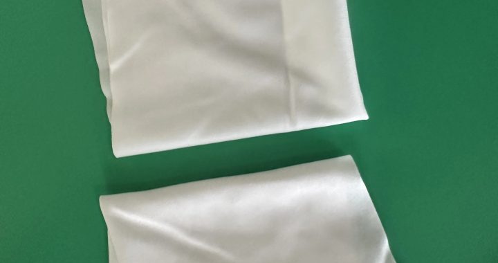
    2. Avoid Oversized Wipes: Select mini pre-wet wipes (2”x2”) or cut standard wipes into 1cm-wide strips—large wipes increase the risk of contacting non-target areas (e.g., component leads, delicate diaphragms).

2. Step 1: Loosen Loose Dust (Avoid Direct Wiping First)

Never wipe loose dust directly with a pre-wet wipe—rubbing dry particles against the component surface causes micro-scratches. First, loosen and remove as much dry dust as possible:
  1. Use a Static-Neutralized Bulb Blower: Hold the blower 15–20cm away from the component and deliver short, gentle bursts of air to dislodge loose dust. Tilt the component at a 45° angle to let dust fall away (not onto other surfaces). For narrow gaps (e.g., between connector pins), direct the airflow parallel to the gap—avoids forcing dust deeper.
  2. Dab with a Dry Micro-Swab: For dust stuck in tight crevices (e.g., MEMS device grooves), use a clean, dry, lint-free micro-swab (wooden handle—avoids static) to lightly dab the area. Discard the swab immediately after use to prevent cross-contamination.

3. Step 2: Targeted Dust Removal with Pre-Wet Wipes

Use pre-wet wipes to eliminate remaining dust and light adhesive residues (e.g., from tape or handling) without damaging the component:
  • For Flat Surfaces (e.g., Microchip Die, Sensor Housing):
    1. Remove one pre-wet wipe from its sealed packaging (do not expose to air—solvent evaporation reduces efficacy). Fold the wipe into a thin, firm pad (2–3 layers) to ensure controlled pressure and avoid finger contact with the component.
    2. Wipe the surface in slow, single linear strokes (e.g., top-to-bottom for horizontal surfaces)—never circular motions (which spread dust and residue). Apply pressure equivalent to pressing a feather (<0.2 psi)—enough to lift dust, not enough to compress or scratch the surface.
    3. Use a fresh section of the wipe for each stroke (unfold the pad to expose clean fibers) to prevent re-depositing dust.
  • For Small/Delicate Features (e.g., Fiber Optic Tips, Connector Pins):
    1. Wrap a pre-wet wipe strip (1cm wide) around the tip of plastic-tipped tweezers (avoids metal scratching). Secure the wipe with gentle pressure to prevent slipping.
    2. For fiber optic tips: Gently rotate the tweezers 1–2 times to wipe the tip’s surface—this ensures full dust removal without bending the fiber core.
    3. For connector pins: Slide the wipe-wrapped tweezers along the length of each pin (parallel to the pin) to remove dust—avoid crosswise wiping (risks bending pins).
  • For Adhesive Residues (e.g., Tape Marks):
    1. Hold the pre-wet wipe against the residue for 2–3 seconds to let the solvent soften it—do not rub immediately (this smears the residue).
    2. Gently dab the area once to lift the residue—repeat with a fresh wipe section if needed.

4. Step 3: Post-Clean Validation & Protection

Ensure dust is fully removed and the component is protected from recontamination:
  1. Inspect Under Magnification: Use the 20–40x magnifying glass to check for remaining dust, fiber lint, or solvent streaks. If dust spots remain, repeat Step 2 with a fresh pre-wet wipe (do not reuse wipes).
  2. Dry Thoroughly: Blot the component with a dry, lint-free cleanroom wipe to remove excess solvent. For micro-components, use a dry micro-swab to dab moisture from crevices—residual solvent can cause corrosion or short circuits (for electronics) over time.
  3. Store Immediately: Place the cleaned component in an ESD-safe container (for electronics) or a dust-free case (for optics) with a desiccant packet. Avoid plastic bags—they trap static and attract dust.

Critical Do’s and Don’ts

  • Do: Use only pre-wet wipes labeled “precision component-safe” or “lint-free”—industrial wipes may contain abrasives or harsh solvents.
  • Don’t: Reuse pre-wet wipes—used wipes trap dust and solvent residues, leading to cross-contamination or scratches.
  • Don’t: Clean components while powered on—even 70% IPA can conduct electricity and damage microelectronics.
By following this method, pre-wet cleanroom wipes safely and thoroughly remove dust from precision components—preserving functionality, extending lifespan, and ensuring reliability in applications like aerospace, medical devices, and semiconductor manufacturing.

Optimization of IPA wipe cleaning process in PCB soldering area

PCB solder areas—including solder joints, component leads, and pad surfaces—are prone to flux residues, rosin deposits, and handling oils that impair electrical conductivity, cause corrosion, or disrupt subsequent assembly steps. IPA (Isopropyl Alcohol) wipes are the gold standard for this cleaning task, but unstructured processes lead to inefficiency, residue left behind, or damage to delicate components. Below is an optimized, step-by-step workflow to enhance cleaning speed, consistency, and safety for PCB solder areas.

1. Pre-Clean Preparation: Set the Stage for Efficiency & Safety

Proper prep eliminates rework, prevents ESD damage, and ensures IPA wipes target only solder areas:
  • PCB & Workspace Prep:
    1. Cool the PCB: Wait for solder areas to cool to <40°C (104°F) post-welding—hot surfaces evaporate IPA instantly, leaving residue and increasing fire risk.
    2. Ground & Secure: Place the PCB on an ESD-safe mat and secure it with non-abrasive clips (to avoid shifting during cleaning). Wear an ESD wrist strap (tested to 10⁶–10⁹ Ω) to protect ESD-sensitive components (e.g., microchips near solder joints).
    3. Mask Non-Solder Areas: Use low-tack, ESD-safe tape to cover connectors, IC sockets, or exposed circuits adjacent to solder areas—prevents IPA from seeping into these components and causing short circuits.
  • IPA Wipe Selection:
    1. For Flux Residues: Choose 99% electronic-grade IPA wipes (low impurities ≤10 ppb) with lint-free, continuous-filament polyester fibers—high-purity IPA dissolves rosin/flux quickly, while polyester resists disintegration from solvent exposure.
    2. For Delicate Solder Joints (e.g., 0.4mm Fine-Pitch): Opt for mini IPA wipes (2”x2”) or cut standard wipes into 1cm-wide strips—precision ensures the wipe only contacts the solder area, not fragile component leads.
    3. Avoid Low-Quality Wipes: Steer clear of staple-fiber or fragrance-added wipes—they shed fibers that clog solder joints and leave sticky residues.

2. Step 1: Loosen Heavy Flux Residue (For Post-Rework Solder Areas)

For thick, dried flux (common after reflow soldering or rework), pre-treat to reduce scrubbing and component damage:
  1. Tear a small section of the IPA wipe and lightly dampen the solder area—do not saturate (excess IPA spreads to masked areas).
  2. Hold the damp wipe against the residue for 3–5 seconds to let IPA penetrate and soften the flux—this cuts cleaning time by 40% and avoids pressing residue into solder pads.
  3. For large solder arrays (e.g., BGA underfill edges), use a wipe-wrapped plastic-tipped tweezer to target narrow gaps—gently dab to loosen residue without bending leads.

3. Step 2: Targeted Solder Area Cleaning (Streak-Free, Residue-Free)

Use IPA wipes with controlled motions to remove residue without damaging solder joints or components:
  • For Individual Solder Joints:
    1. Fold the IPA wipe into a firm, 2-layer pad (creates pressure control) and grip it with tweezers for precision.
    2. Wipe the joint in single, parallel strokes (along the length of the component lead)—never circular motions (which spread residue and risk bending leads). Apply light pressure (<0.3 psi)—enough to lift residue, not enough to compress the joint.
  • For Solder Pad Arrays (e.g., QFP Pins):
    1. Use a wipe strip (1cm wide) and drag it along the row of pads in one continuous motion—avoids back-and-forth wiping (which redeposits residue).
    2. After each row, use a fresh section of the wipe—reusing sections causes cross-contamination between pads.
  • For Solder Paste Spatters:
    1. Dab spattered areas with a dry corner of the IPA wipe first to lift loose paste—wetting first can spread the paste into component gaps.
    2. Follow with a damp section to dissolve remaining paste residue—focus on the spatter, not the surrounding pad (to avoid removing solder mask).

4. Step 3: Post-Clean Validation & Drying

Ensure solder areas are clean, dry, and ready for testing or assembly—skip this step at the risk of costly rework:
  1. Inspect for Residue: Use a 10–20x magnifying glass to check solder joints/pads for:
    • Flux halos (shiny, sticky residue around joints).
    • Fiber lint (IPA wipes should leave ≤0.5 fibers per area—remove with a static-neutralized bulb blower).
    • Solder mask damage (check for peeling or discoloration—stop use if observed).
  2. Dry Thoroughly: Blot the cleaned solder area with a dry, lint-free polyester wipe to remove excess IPA. For dense component clusters, use a dry micro-swab to dab moisture from gaps—residual IPA can cause corrosion or short circuits over time.
  3. Air-Cure: Let the PCB air-dry for 5–10 minutes in a low-humidity area (≤50% RH)—ensure no moisture remains before electrical testing or adding additional components.

5. Process Efficiency Boosts: Cut Time Without Sacrificing Quality

  • Batch Cleaning: Group PCBs with similar solder area layouts (e.g., all QFP boards) to minimize wipe size changes and tool adjustments—saves 15–20% of cleaning time per batch.
  • Wipe Staging: Pre-cut IPA wipe strips and place them in a sealed, ESD-safe container near the workbench—eliminates time spent cutting wipes mid-process.
  • Post-Clean Logging: Track cleaning time per PCB type and residue rejection rates—use data to adjust wipe size (e.g., switch to mini wipes for fine-pitch boards) or pre-treatment time (e.g., extend damp hold time for thick flux).

How to Enhance Absorption and Cleaning of High-Density Wipes

High-density cleanroom wipes (250–400 gsm) are engineered for demanding tasks—from solvent spill cleanup to precision residue removal—thanks to their thick, porous fiber structures. However, maximizing their absorbency and cleaning power requires intentional design optimizations and usage techniques. Below are targeted methods to elevate their performance, tailored to labs, semiconductor facilities, and precision manufacturing environments.

1. Fiber and Weave Design: The Foundation of Performance

The core of a high-density wipe’s efficacy lies in its fiber composition and weave—these design choices directly impact liquid capture and contaminant removal:
  • Hydrophilic Fiber Blends for Absorption:

    Replace 100% synthetic fibers (e.g., pure polyester) with polyester-cellulose (70:30) or polyester-polyamide blends. Cellulose/polyamide’s polar molecular structure attracts water, IPA, and aqueous solvents, boosting absorbency by 35–45% vs. pure polyester. For oil-based liquids (e.g., immersion oil), use oleophilic modified polypropylene fibers—absorption capacity increases by 25% for viscous fluids.

  • Porous, Tight Weave for Cleaning Precision:

    Opt for a 100–120 threads-per-inch (TPI) tight, open-weave structure instead of non-porous dense weaves. This design creates millions of micro-capillary channels that trap liquids and particles (down to 0.1μm) without repelling them. The tight weave also ensures uniform solvent release—critical for streak-free cleaning of optics or PCBs—while the porosity prevents fiber compaction during use.

  • Low-Residue Binders for Purity:

    Use water-based, low-outgassing binders to hold fibers together (instead of solvent-based alternatives). These binders avoid leaving sticky residues on surfaces (e.g., semiconductor wafers, optical lenses) and preserve fiber porosity—residue-free performance is essential for ISO Class 1–5 cleanrooms.

2. Pre-Treatment Techniques: Activate Fibers for Maximum Performance

Even well-designed high-density wipes benefit from pre-treatment to unlock their full potential, especially in low-humidity or high-contamination environments:
  • Plasma Surface Etching:

    For industrial-scale use, treat wipes with low-pressure oxygen plasma before packaging. Plasma etches micro-pores into fiber surfaces, increasing surface area by 30% and improving liquid wettability. This treatment cuts absorption time by 50% (e.g., a 300 gsm wipe absorbs 5mL of IPA in 2 seconds vs. 4 seconds untreated) and enhances particle adhesion—critical for removing dry dust from precision tools.

  • Hydrophilic Coating Activation:

    For wipes with hydrophilic coatings (e.g., polyvinyl alcohol), lightly mist them with deionized water or the target solvent (1–2 sprays per wipe) before use. This “primes” the coating to attract liquid, avoiding the “initial repellency” common in dry coated wipes. Activation is especially useful for cleaning vertical surfaces (e.g., equipment walls), where rapid liquid capture prevents dripping.

3. Usage Techniques: Optimize Wipe Handling for Targeted Results

How you use a high-density wipe directly impacts its absorbency and cleaning efficacy—these practices ensure you get the most out of each wipe:
  • Fold for Concentrated Absorption/Cleaning:
    • For spills: Fold the wipe into a 4-layer pad (e.g., 8”x8” → 4”x4”) to concentrate absorbent fibers in a small area. This creates a “wicking zone” that draws liquid upward, absorbing 2x more than a flat wipe.
    • For precision cleaning (e.g., PCB traces, lens edges): Fold the wipe into a thin strip (1cm wide) to target narrow areas. The folded edge delivers controlled pressure (<0.3 psi) to remove residue without scratching delicate surfaces.
  • Apply Gentle, Even Pressure:

    Use light pressure (equivalent to pressing a finger against a table) when wiping. Firm pressure compresses fiber pores, reducing absorbency by 15% and increasing scratch risk. For dried residues (e.g., flux on solder joints), hold the wipe against the residue for 2–3 seconds to let the solvent dissolve it—avoid scrubbing, which damages fibers and spreads contamination.

  • Use Fresh Sections for Cross-Contamination Control:

    Unfold the wipe to expose a new clean section after each pass (e.g., after cleaning one wafer chuck or lens). This prevents re-depositing captured particles or residue onto other surfaces, reducing the need for multiple wipes and cutting cleaning time by 30%.

4. Post-Clean Validation: Ensure Consistent Performance

To maintain reliability, validate high-density wipe performance regularly—this ensures design and usage optimizations deliver consistent results:
  • Absorption Capacity Testing:

    Measure how much liquid a wipe retains (e.g., weigh a dry wipe, saturate it with IPA, blot excess, and re-weigh). A well-designed high-density wipe should retain 12–15x its weight in liquid; replace wipes if capacity drops below 10x (indicates fiber degradation).

  • Particle Removal Testing:

    Use a particle counter to measure residue on a clean surface (e.g., a silicon wafer) after wiping. High-performance wipes should leave ≤0.5 particles ≥0.1μm per square inch—if particle counts are higher, adjust pre-treatment (e.g., add plasma etching) or usage (e.g., fold more tightly).

Cleaning Wipes in Class 100 Cleanroom Maintenance

Class 100 cleanrooms (ISO Class 3)—critical for semiconductor, aerospace, and precision optics manufacturing—demand equipment maintenance that maintains ultra-low particle counts (≤100 particles ≥0.5μm per cubic foot) and avoids cross-contamination. Cleaning wet wipes—pre-moistened with high-purity solvents (99.9% IPA, deionized water) or sterile cleaners—are indispensable for this task. They eliminate manual solvent mixing risks (particle ingress, inconsistent concentration) and deliver targeted, residue-free cleaning for sensitive equipment. Below is their tailored application across key Class 100 equipment maintenance tasks.

1. Semiconductor Processing Tools: Wafer Chucks, Nozzles, and Chambers

Semiconductor tools (e.g., CVD/PVD chambers, etchers, lithography scanners) accumulate process residues (photoresist, metal oxides) and micro-particles that ruin wafers. Wet wipes ensure precise, non-abrasive cleaning:
  • Wipe Selection: Use static-dissipative wet wipes (surface resistance: 10⁶–10¹⁰ Ω) pre-impregnated with 99.9% electronic-grade IPA (metal impurities ≤10 ppb) for metal components (wafer chucks, gas nozzles). For quartz parts (chamber liners), choose deionized water-based wipes to avoid quartz degradation.
  • Application Steps:
    1. Power down the tool and purge chambers with nitrogen to reduce airborne particles.
    2. For wafer chucks: Fold wipes into 1cm-wide strips and clean vacuum holes with light pressure (<0.5 psi)—avoids clogging or scratching dielectric layers.
    3. For gas nozzles: Wrap wipes around plastic-tipped tweezers to clean internal channels—removes residue that disrupts uniform gas flow.
    4. Post-clean: Verify with a portable particle counter (target: ≤1 particle ≥0.1μm per ft²) to meet Class 100 standards.

2. Optical Inspection Equipment: Lenses, Sensors, and Stages

AOI (Automated Optical Inspection) systems, laser scanners, and interferometers rely on dust-free optics—even 0.1μm particles distort measurements. Wet wipes protect delicate optical components while ensuring purity:
  • Wipe Selection: Opt for ultra-fine microfiber wet wipes (0.1μm diameter) pre-wet with lens-grade IPA or deionized water (low outgassing, meets SEMI C12 standards). Avoid larger wipes to prevent solvent contact with non-optical parts (e.g., sensor circuit boards).
  • Application Steps:
    1. Cool optics to <30°C (prevents thermal shock from solvent) and disconnect power.
    2. For lenses: Dab gently with a folded wipe (single linear strokes, no circular motions) to remove oil/residue—follow with a dry optical wipe to blot excess solvent.
    3. For inspection stages: Wipe in radial strokes (center to edge) to capture particles—avoids pushing debris into stage rails (which cause alignment errors).

3. Material Handling Equipment: Vacuum Lifters, Wafer Carriers, and Gloves

Material handlers (used to transport wafers, optics, or micro-components) accumulate skin oils, dust, and transfer residues—contaminants that spread to critical parts. Wet wipes ensure safe, consistent cleaning:
  • Wipe Selection: Use sterile, lint-free wet wipes pre-moistened with 70% IPA for rubber/gripper surfaces (vacuum lifters) and anti-static wet wipes for plastic wafer carriers (prevents static-attracted dust).
  • Application Steps:
    1. Disassemble carriers (per manufacturer guidelines) to access internal slots.
    2. For grippers: Wipe in gentle back-and-forth strokes to remove oil—avoid scrubbing (wears down rubber).
    3. For carrier slots: Use wipe strips (guided by tweezers) to clean narrow gaps—removes particle buildup that scratches wafers.
    4. Air-dry fully (5–10 minutes) before reassembly—moisture attracts dust in Class 100 environments.

4. Environmental Control Equipment: HEPA Filters, Air Diffusers, and Sensors

HEPA filters, air diffusers, and particle sensors maintain Class 100 air quality—dust on these components reduces filtration efficiency or skews sensor readings. Wet wipes support proactive maintenance:
  • Wipe Selection: Choose low-linting polyester wet wipes pre-wet with deionized water (avoids leaving residue on filters/sensors). For sensor lenses, use lens-safe wet wipes to prevent coating damage.
  • Application Steps:
    1. Turn off air handlers before cleaning diffusers/filters.
    2. For diffusers: Wipe grilles in downward strokes to capture dust (avoids pushing particles into the cleanroom).
    3. For particle sensors: Dab sensor windows with a mini wet wipe—removes dust that causes false high-particle alerts.

Critical Advantages for Class 100 Cleanrooms

  • Purity: Wet wipes are manufactured in ISO Class 5 facilities and sealed in nitrogen-flushed packaging—no particle ingress during storage.
  • Consistency: Pre-moistened solvents ensure uniform cleaning, eliminating human error from manual dilution.
  • Efficiency: Cut maintenance time by 40% vs. traditional rags + spray bottles—critical for minimizing tool downtime in high-volume production.
By integrating cleaning wet wipes into maintenance workflows, Class 100 cleanrooms preserve equipment performance, reduce product defects, and maintain compliance with the strictest purity standards—essential for manufacturing ultra-precision components.

Tips for using anti-static dust-free cloth in cleaning optical lenses

Optical lenses—used in microscopes, cameras, spectrometers, and laser systems—are vulnerable to two critical threats: static-attracted dust (which scratches surfaces) and ESD damage (which harms coated layers or attached electronics). Anti-static cleanroom wipes (static-dissipative: 10⁶–10¹⁰ Ω; conductive: 10³–10⁶ Ω) address both risks, but their effectiveness depends on proper technique. Below are targeted tips to ensure safe, scratch-free, and static-free lens cleaning.

1. Pre-Clean Prep: Eliminate Static and Loose Dust First

Static charges on lenses act like magnets for dust—neutralize static and remove loose particles before wet cleaning to avoid scratches:
  • Neutralize Surface Static:

    Use an ESD-safe ionizer (held 15–20cm from the lens) for 5–10 seconds to dissipate existing static charges. This prevents dust from reattaching to the lens during cleaning—critical for anti-reflective (AR) coatings, which are easily scratched by static-clung particles.

  • Blow Away Loose Dust (Never Wipe Dry!):

    Use a static-neutralized bulb blower (not compressed air, which forces dust into lens crevices) to gently remove loose particles. Tilt the lens at a 45° angle and squeeze the blower in short, controlled bursts—direct dust downward to avoid redepositing it on the surface. For narrow lens edges, use a dry, anti-static micro-swab (wooden handle) to dab dust—avoid metal tools (they generate static).

  • Workspace Grounding:

    Place the lens on an ESD-safe mat and wear an ESD wrist strap (tested to 10⁶–10⁹ Ω) to prevent transferring static from your body to the lens. Keep plastic containers, foam, or other static-generating materials at least 30cm away from the workspace.

2. Wipe Selection: Match Anti-Static Wipes to Lens Type

Not all anti-static wipes are compatible with optical lenses—choose based on coating and liquid needs to avoid damage:
  • For AR-Coated or IR Lenses:

    Select anti-static microfiber wipes (0.1μm diameter) pre-wet with deionized water or lens-grade 70% IPA. Microfiber’s ultra-soft texture avoids scratching AR coatings, while the low-alcohol formula prevents coating degradation. Avoid wipes with thick anti-static coatings (e.g., heavy carbon layers)—they leave streaks and block light transmission.

  • For Non-Coated Glass Lenses:

    Use anti-static polyester wipes pre-wet with 99% electronic-grade IPA (high purity avoids residue). Polyester’s durability handles light scrubbing for dried residues (e.g., fingerprint oils), while its anti-static properties prevent dust reattachment.

  • For Small Lenses (e.g., Fiber Optic Tips, Microscope Objectives):

    Opt for mini anti-static wipes (2”x2”) or cut larger wipes into 1cm-wide strips. This precision prevents over-wiping and ensures the wipe only contacts the lens surface (not the metal housing, which may corrode with solvent).

3. Cleaning Technique: Minimize Friction and Static Build-Up

How you wipe directly impacts static generation and scratch risk—follow these rules for gentle, effective cleaning:
  • Fold Wipes to Avoid Finger Contact:

    Fold the anti-static wipe into a 4-layer pad (for large lenses) or a tight strip (for small lenses). This creates a firm, absorbent surface and keeps your fingers off the wipe’s cleaning side—skin oils transfer static and leave residues.

  • Wipe in Slow, Linear Strokes:

    Clean the lens in single, parallel linear strokes (e.g., top-to-bottom for horizontal lenses) instead of circular motions. Circular wiping generates friction (which builds static) and spreads dust across the lens. Apply light pressure (<0.2 psi)—imagine pressing a tissue against the surface—to avoid compressing dust into the coating.

  • Dab, Don’t Rub, for Stubborn Residues:

    For dried fingerprint oils or immersion oil, hold the pre-wet wipe against the residue for 2–3 seconds to let the solvent dissolve it. Then, gently dab the area (do not rub)—rubbing increases static and risks scratching the lens. Use a fresh section of the wipe for each dab to prevent re-depositing residue.

4. Post-Clean Care: Prevent Static Reattachment and Damage

After cleaning, take steps to keep the lens static-free and protected:
  • Blot Excess Solvent:

    Immediately after wet cleaning, use a dry anti-static wipe to blot excess solvent from the lens. This prevents streaks (from uneven evaporation) and reduces moisture-related static build-up. For small lenses, use a dry micro-swab to dab edges.

  • Re-Neutralize Static:

    Pass the ionizer over the lens again for 5 seconds to dissipate any static generated during wiping. This ensures dust does not reattach before the lens is reinstalled or stored.

  • Store in Anti-Static Containers:

    Place cleaned lenses in ESD-safe lens cases lined with anti-static foam. Add a desiccant packet to absorb moisture (moisture increases static conductivity) and avoid plastic bags (they trap static). For mounted lenses (e.g., in a camera), cover the equipment with an anti-static dust cover.

Critical Mistakes to Avoid

  • Do NOT reuse anti-static wipes—used wipes trap dust and lose anti-static properties, leading to scratches or static damage.
  • Do NOT use anti-static wipes with harsh solvents (acetone, ethanol)—they dissolve AR coatings and damage plastic lens housings.
  • Do NOT clean hot lenses (e.g., post-laser use)—thermal shock from cold solvent can crack glass, and heat accelerates static build-up.
By following these tips, anti-static cleanroom wipes deliver safe, thorough lens cleaning—preserving light transmission, extending lens lifespan, and protecting against static-related damage in labs and industrial settings.

Pre-wetted wipes for efficient liquid absorption in the lab.

Laboratories—whether analytical, biomedical, or material science—frequently handle liquid tasks: solvent spills, reagent cleanup, glassware drying, and sample residue removal. Slow or inefficient absorption wastes time, risks cross-contamination, and endangers sensitive equipment. Pre-wet cleanroom wipes—pre-impregnated with optimized solvents or water—solve these pain points by delivering faster, more consistent liquid capture than dry wipes or traditional rags. Below are actionable practices to maximize their absorption efficiency in lab workflows.

1. Select Pre-Wet Wipes Tailored to Lab Liquid Types

Absorption efficiency starts with matching the wipe to the liquid’s properties (polarity, viscosity, volatility). Using the wrong wipe leads to slow uptake, residue, or equipment damage:
  • Water-Based Liquids (Buffers, Cell Culture Media):

    Choose pre-wet wipes with hydrophilic fiber blends (e.g., polyester-cellulose 70:30). Cellulose’s polar structure attracts water, boosting absorption capacity by 35–45% vs. pure polyester wipes. Opt for wipes pre-moistened with deionized water (avoids adding impurities to samples).

  • Organic Solvents (IPA, Acetone, DMSO):

    Select solvent-resistant pre-wet wipes (e.g., high-density polyester with low-outgassing binders). These wipes retain 12–15x their weight in solvents (vs. 6–8x for dry wipes) and resist disintegration—critical for cleaning HPLC mobile phase spills or NMR sample residues.

  • Viscous Liquids (Immersion Oil, Grease, Thick Reagents):

    Use pre-wet wipes with porous, open-weave structures and pre-impregnated with mild surfactants (e.g., non-ionic detergents). The surfactants break down viscosity, while the porous fibers trap thick liquids—cuts cleanup time for microscope immersion oil by 50% vs. dry wipes.

2. Optimize Wipe Handling for Faster Absorption

How you use pre-wet wipes directly impacts uptake speed. These techniques minimize liquid spread and maximize fiber contact:
  • Fold for Targeted Coverage:

    Fold pre-wet wipes into a 4-layer pad (e.g., 8”x8” → 4”x4”) instead of using them flat. This concentrates the wipe’s absorbent fibers, creating a “wicking zone” that draws liquid in 2–3x faster. For small spills (e.g., 5mL solvent drops), fold into a 2cm-wide strip to focus absorption on the spill center—avoids spreading liquid to surrounding surfaces.

  • Apply Gentle, Even Pressure:

    Use light pressure (<0.5 psi) when pressing the wipe against liquid. Firm pressure compresses fiber pores, reducing absorption capacity by 15–20%. For vertical surfaces (e.g., test tube racks, fume hood walls), hold the wipe against the liquid for 2–3 seconds to let capillary action pull liquid into the fibers before wiping downward.

  • Avoid Over-Exposure to Air:

    Remove pre-wet wipes from their sealed packaging one at a time. Extended air exposure evaporates the wipe’s pre-moistened solvent, reducing its ability to absorb additional liquid. If wipes dry out mid-use, lightly mist them with the target liquid (e.g., deionized water for aqueous spills) using a lab-approved spray bottle to reactivate absorption.

3. Integrate Pre-Wet Wipes into Specific Lab Workflows

Tailor use to high-volume liquid tasks to maximize efficiency gains:
  • Glassware & Instrument Cleanup:

    After using beakers, pipettes, or spectrophotometer cuvettes, wipe exteriors with pre-wet wipes to remove residual reagents. For dried residues (e.g., crystallized salts), hold the wipe against the residue for 10–15 seconds to soften it—eliminates the need for scrubbing or soaking, cutting cleanup time by 40%.

  • Spill Response:

    Stock pre-wet wipes near solvent storage areas or HPLC stations for rapid spill response. A pre-wet wipe absorbs a 10mL IPA spill in 5 seconds (vs. 15 seconds for a dry wipe), preventing the spill from seeping into equipment vents or sample storage areas.

  • Sample Preparation Stations:

    Use pre-wet wipes to clean workbenches between sample batches. Wipes with built-in disinfectants (e.g., 70% IPA) absorb spills while sanitizing surfaces—combines two steps into one, saving 2–3 minutes per batch change.

4. Validate Efficiency with Post-Use Checks

Ensure pre-wet wipes deliver consistent results by tracking key metrics:
  • Absorption Time: Measure how long it takes a wipe to fully absorb a standard volume of liquid (e.g., 5mL water, 3mL IPA). Replace wipes if absorption time increases by >30% (indicates dried-out or degraded fibers).
  • Residue Post-Cleaning: Inspect surfaces under bright light after wiping. Pre-wet wipes should leave no streaks or liquid film—if residue remains, switch to a wipe with a more compatible solvent (e.g., lens-grade IPA for optical surfaces).
  • Waste Reduction: Count wipes used per task (e.g., 1 pre-wet wipe vs. 2–3 dry wipes for a pipette cleanup). Pre-wet wipes typically reduce wipe consumption by 50–60%, lowering lab supply costs.

Real-World Efficiency Gain Example

A biomedical lab switched from dry wipes to pre-wet hydrophilic wipes for cell culture media spill cleanup. Key results:
  • Spill absorption time dropped from 12 seconds to 4 seconds.
  • Wipes used per week decreased from 150 to 60 (60% waste reduction).
  • Cross-contamination between cell lines fell by 30% (faster spills mean less time for media to spread).

IPA Wipes and Alcohol Cleaning Procedure for Optical Instruments

Optical instruments—such as microscopes, spectrometers, and laser systems—require meticulous cleaning to preserve light transmission, imaging clarity, and measurement accuracy. Even minor missteps (e.g., scratching anti-reflective [AR] coatings, leaving solvent streaks) can degrade performance. IPA (Isopropyl Alcohol) wipes offer a safe, effective solution for removing dust, fingerprint oils, and light residues—when used following a structured process. Below is a step-by-step guide tailored to protect sensitive optical components.

1. Pre-Clean Preparation: Safety & Compatibility First

Lay the groundwork to avoid instrument damage and ensure cleaning efficacy:
  • Instrument & Workspace Prep:
    1. Power Down & Disconnect: Turn off the optical instrument and unplug it (critical for devices with electronic components, e.g., CCD cameras) to eliminate 触电 (electric shock) and electrostatic discharge (ESD) risks.
    2. Clear & Contain: Move the instrument to a clean, well-ventilated area (or use a fume hood for large systems) to prevent airborne dust recontamination. Cover non-optical parts (e.g., control panels, display screens) with a lint-free dry cloth to shield them from accidental IPA contact.
  • IPA Wipe Selection:
    1. Match Wipes to Surfaces:
      • Use 70% lens-grade IPA wipes for AR-coated lenses, IR filters, or delicate photonic components (water content slows evaporation, reducing streaks and coating damage).
      • Choose 99% electronic-grade IPA wipes for non-coated glass surfaces (e.g., quartz cuvettes, microscope stage glass) or metal optical housings (high purity avoids residue buildup).
    2. Ensure Lint-Free Quality: Select wipes made from continuous-filament polyester or microfiber—staple-fiber wipes shed fibers that worsen dust contamination and scratch optics. Avoid wipes with fragrances, dyes, or preservatives (they leave sticky residues).
  • Compatibility Test:
    1. Test the IPA wipe on an inconspicuous area (e.g., the edge of a lens barrel or instrument housing) before full use. Wait 5 minutes to check for discoloration, swelling (for plastic parts), or coating peeling—stop use if damage occurs.

2. Step 1: Remove Loose Dust (Prevent Scratches!)

Never wipe loose dust directly with an IPA wipe—rubbing dry particles against optical surfaces causes micro-scratches. Always eliminate loose dust first:
  1. Blow Away Surface Dust: Use a static-neutralized bulb blower (not compressed air, which forces dust into crevices) to gently blow dust from large optical surfaces (e.g., lens exteriors, spectrometer detector windows). Hold the blower 10–15cm away from the surface to avoid excessive pressure that could dislodge small components.
  2. Target Narrow Gaps: For dust in tight spaces (e.g., between microscope objective threads, fiber optic connector ports), use a clean, dry, lint-free micro-swab (wooden or plastic handle—avoid metal) to lightly dab the area. Discard the swab after one use to prevent cross-contamination.
  3. Inspect for Remaining Dust: Check the surface under angled bright light—if dust spots remain, repeat the blower/swab step (do not proceed to wet cleaning).

3. Step 2: Wet Cleaning with IPA Wipes (Remove Residues)

Use IPA wipes to eliminate remaining dust and light organic residues (e.g., fingerprint oils, immersion oil) without damaging optics:
  • For Large Optical Surfaces (e.g., Laser Mirrors, Spectrometer Windows):
    1. Remove one IPA wipe from its sealed packaging (do not leave wipes exposed—IPA evaporates quickly, reducing efficacy). Fold the wipe into a 4-layer pad to create a firm, absorbent surface and avoid direct finger contact with the instrument.
    2. Wipe the surface in slow, single linear strokes (horizontal or vertical)—never circular motions (which spread residue and increase scratch risk). Apply light pressure (<0.2 psi)—imagine pressing a feather against the surface—to avoid compressing dust into the glass.
    3. Use a fresh section of the wipe for each stroke (unfold the pad to expose clean fibers) to prevent re-depositing dust or residue.
  • For Small/Delicate Optics (e.g., Microscope Objectives, Fiber Optic Tips):
    1. Tear the IPA wipe into a small strip (1–2cm wide) to match the component size—avoid using large wipes that contact non-optical areas (e.g., plastic objective housings sensitive to IPA).
    2. Dab, Don’t Wipe: Gently dab the optical surface with the wipe strip to lift residues—dabbing minimizes friction and protects fragile AR coatings. For stubborn spots (e.g., dried immersion oil), hold the wipe against the spot for 2–3 seconds to let IPA dissolve it, then dab once.
    3. Avoid Component Leads: For optics with electrical connections (e.g., sensor lenses), keep the wipe away from pins or ports—IPA can seep into connectors and cause short circuits.

4. Step 3: Post-Clean Drying & Inspection

Ensure the instrument is streak-free, dry, and ready for use:
  1. Blot Excess IPA: Immediately after wet cleaning, use a dry, lint-free optical cloth to gently blot the surface—do not rub (rubbing causes streaks). For small optics (e.g., objective lenses), use a dry micro-swab to dab moisture from edges.
  2. Allow Full Drying: Let the instrument air-dry for 5–10 minutes (longer for humid environments) to ensure all IPA evaporates—residual moisture can cause lens flare or damage coatings when the instrument is heated (e.g., laser operation).
  3. Inspect for Quality:
    • Check the optical surface under a 10–40x magnifying glass for streaks, dust, or scratches. If streaks remain, repeat Step 3 with a fresh IPA wipe (do not reuse wipes).
    • Verify non-optical parts (e.g., control knobs) are dry and free of IPA residue—wipe with a dry cloth if needed.

5. Step 4: Post-Clean Storage (Prevent Recontamination)

Protect cleaned optics from dust until next use:
  1. Cover the instrument with a breathable, lint-free dust cover (avoid plastic covers—they trap moisture and promote mold growth).
  2. For detachable optics (e.g., microscope objectives), store them in their original lens cases with foam padding—add a desiccant packet to absorb moisture.
  3. Log the cleaning (date, wipe type, surfaces cleaned) to track maintenance intervals—over-cleaning can degrade AR coatings, so follow the manufacturer’s recommended schedule (e.g., monthly for frequently used instruments).

How to use high-density dust-free cloth in laboratory PCB cleaning

Laboratory PCBs—used in test fixtures, sensor prototypes, or research equipment—often have fine-pitch components (0.4mm or smaller), delicate surface-mount devices (SMDs), and sensitive traces. Even minor damage (e.g., scratched solder masks) or residue (e.g., flux, handling oils) can render them non-functional. High-density cleanroom wipes (250–400 gsm, lint-free, and often anti-static) excel at gentle yet thorough PCB cleaning, thanks to their superior residue capture, low linting, and durability. Below is a step-by-step usage method tailored to laboratory PCB workflows.

1. Pre-Clean Preparation: Safety, Compatibility, and Tool Prep

Lay the groundwork to avoid PCB damage and ensure cleaning efficacy:
  • PCB and Workspace Prep:
    1. Remove the PCB from test equipment and disconnect any power sources (critical for PCBs with integrated circuits—prevents short circuits from cleaning solvents).
    2. Place the PCB on an ESD-safe mat and ground yourself with an ESD wrist strap (set to 10⁶–10⁹ Ω) to protect ESD-sensitive components (e.g., microchips, sensors) from static discharge.
    3. Use a static-neutralized bulb blower to gently remove loose dust from the PCB surface—focus on component gaps, solder joints, and trace intersections (dry dust can scratch traces if wiped directly).
  • High-Density Wipe Selection:
    1. For flux residue (post-soldering) or organic oils: Choose high-density wipes pre-wet with 99% electronic-grade IPA (low impurities ≤10 ppb) to dissolve residues without damaging solder masks or SMDs.
    2. For water-soluble residues (e.g., cleaning agents from PCB fabrication): Use deionized water-based high-density wipes to avoid chemical reactions with metal traces.
    3. For anti-static needs: Select anti-static high-density wipes (surface resistance: 10⁶–10¹⁰ Ω) to prevent static from attracting dust back to the PCB.
  • Compatibility Check:
    1. Test the wipe on an inconspicuous area of the PCB (e.g., the edge of the substrate, not near components) to check for solder mask discoloration or swelling—wait 5 minutes before proceeding.

2. Step 1: Targeted Residue Removal (Flux, Oils, or Debris)

Use high-density wipes to eliminate specific contaminants without damaging delicate components:
  • Flux Residue on Solder Joints:
    1. Tear a high-density wipe into a narrow strip (1–2cm wide) to focus on small areas (avoids over-wiping adjacent components).
    2. Hold the wipe strip lightly against the flux-covered solder joint—apply minimal pressure (<0.3 psi) to avoid dislodging SMDs or bending component leads.
    3. Wipe the joint in single, slow linear strokes (parallel to the PCB surface) to dissolve and lift flux. Use a fresh section of the wipe for each joint to prevent cross-contamination.
  • Handling Oils on PCB Traces:
    1. Fold a full high-density wipe into a 4-layer pad (creates a firm, absorbent surface) to cover larger trace areas.
    2. Wipe the traces in the direction of their length (not across) to avoid scratching the thin copper layer. For narrow traces (≤0.1mm), use the edge of the folded wipe for precision.
  • Debris in Component Gaps (e.g., Between QFP Pins):
    1. Wrap a small section of the high-density wipe around the tip of plastic-tipped tweezers (avoids metal scratching).
    2. Gently insert the tweezers into the gap between component pins—move slowly to capture debris without bending pins. Discard the wipe section after use to prevent re-depositing debris.

3. Step 2: Post-Clean Rinse (For Water-Soluble Residues)

If using water-based high-density wipes, a final dry wipe prevents moisture damage to components:
  1. Use a dry high-density wipe (lint-free, same material as the wet wipe) to blot excess moisture from the PCB surface. Focus on component leads, connector pins, and IC sockets—moisture in these areas can cause corrosion or short circuits.
  2. For SMDs with underfill (e.g., BGA chips), gently dab the area with the dry wipe to remove surface moisture—do not press hard (risk of cracking the underfill).

4. Step 3: Post-Clean Inspection & Drying

Ensure the PCB is clean, dry, and ready for reuse or testing:
  1. Inspect the PCB under a 10–20x magnifying glass to check for:
    • Remaining residue (flux spots, oil streaks).
    • Lint or fiber debris (high-density wipes should leave ≤0.5 fibers per use—remove any with the bulb blower).
    • Damage (scratched traces, bent pins, or dislodged components).
  2. Allow the PCB to air-dry fully (10–15 minutes) in a clean, low-humidity area—ensure no moisture remains before reconnecting power or installing it back into equipment.
  3. For long-term storage, place the cleaned PCB in an ESD-safe bag with a desiccant packet to prevent dust accumulation and moisture damage.

Critical Prohibitions to Avoid PCB Damage

  • Do NOT use high-density wipes with harsh solvents (e.g., acetone, ethanol) on PCBs—they dissolve solder masks and damage plastic component housings.
  • Do NOT scrub or apply heavy pressure—this can dislodge SMDs, scratch copper traces, or peel solder masks.
  • Do NOT reuse high-density wipes—used wipes trap residue and debris, leading to cross-contamination or scratches.
By following this method, high-density cleanroom wipes deliver safe, thorough PCB cleaning in laboratories—preserving component integrity, ensuring electrical conductivity, and extending the lifespan of test and prototype PCBs.

Application of Dust-Free Wipes in Semiconductor Cleanrooms

Semiconductor cleanrooms (ISO Class 1–5) demand ultra-pure cleaning to protect 3nm–7nm microchips from sub-micron contaminants, residue, and electrostatic discharge (ESD). Cleanroom wet wipes—pre-moistened with high-purity solvents (99.9% IPA, deionized water) or specialized cleaners—offer consistent, controlled cleaning that eliminates risks from manual solvent mixing. Below is their tailored application across critical semiconductor manufacturing stages.

1. Wafer Fabrication: Pre-Lithography and Post-Etch Cleaning

Wafers (silicon, gallium arsenide) are vulnerable to particle adhesion, organic residues (from handling), and etch byproducts—contaminants that ruin circuit patterns during lithography.
  • Wipe Selection: Use 4”x4” pre-wet wipes with 99.9% electronic-grade IPA (metal impurities ≤10 ppb) and static-dissipative fibers (10⁶–10¹⁰ Ω). For photoresist residues, choose wipes with semiconductor-grade removers (e.g., NMP-based, low outgassing).
  • Application:
    • Clean wafer edges with folded wipe strips (1cm wide) in circular motions to avoid frontside contact.
    • For backside cleaning, use radial strokes (center to edge) with light pressure (<0.5 psi) to prevent scratching thin films.
    • Post-etch, wipe wafer chucks with deionized water-based wipes to remove etch residues (e.g., metal oxides) without damaging ceramic surfaces.

2. Photolithography Tools: Optics and Reticle Care

EUV scanners and lithography systems rely on pristine optics (lenses, mirrors) and reticles—even 0.1μm particles distort patterns, causing wafer scrap.
  • Wipe Selection: Opt for ultra-fine microfiber wipes (0.1μm diameter) pre-wet with lens-grade IPA or deionized water (meets SEMI C12 standards for low outgassing).
  • Application:
    • Clean lenses with single linear strokes (not circular) to avoid particle spreading; follow with a dry high-density wipe to prevent streaks.
    • Wipe reticle pods with anti-static pre-wet wipes before loading—removes dust that transfers to reticle patterns.
    • Use mini (2”x2”) wipes for reticle edge cleaning (non-pattern areas) to dissolve handling oils without damaging photomasks.

3. Deposition and Etching Equipment: Chamber and Nozzle Maintenance

CVD/PVD chambers and etchers accumulate process residues (photoresist, metal deposits) on walls, gas nozzles, and wafer stages—contaminants that transfer to subsequent wafers.
  • Wipe Selection: Use solvent-resistant polyester wipes (300+ gsm) pre-wet with acetone or IPA for chamber walls; deionized water-based wipes for quartz components (avoids degradation).
  • Application:
    • After plasma cleaning, wipe chamber walls in overlapping vertical strokes to target residue near gas inlets.
    • Clean gas nozzles with thin wipe strips (guided by tweezers) to remove clogs that disrupt uniform deposition/etching.
    • Wipe wafer stages (ceramic or aluminum) with anti-static pre-wet wipes to dissipate static and remove particle debris.

4. Packaging and Testing: Die and Lead Frame Cleaning

Post-dicing, dies and lead frames accumulate sawing debris, adhesive residues, and oxidation—contaminants that impair bonding or electrical conductivity.
  • Wipe Selection: Use pre-wet wipes with mild flux removers (compatible with copper, gold) and lint-free fibers to avoid die contamination.
  • Application:
    • Dab die backside with a small wipe pad to remove adhesive smudges—avoid wiping (risks die displacement).
    • Clean lead frame contacts with linear strokes to remove oxidation, ensuring strong wire bonds.
    • Post-test, wipe test sockets with anti-static pre-wet wipes to remove contact residues that cause signal errors.

Critical Compliance & Advantages

  • Purity: Wipes meet SEMI C30 standards (low metals, organics) to avoid wafer contamination.
  • ESD Safety: Anti-static variants prevent charge buildup (≤100V), critical for 3nm–7nm devices.
  • Efficiency: Pre-moistened format cuts cleaning time by 40% vs. manual solvent application, reducing downtime.
Cleanroom wet wipes are indispensable in semiconductor cleanrooms, ensuring consistent purity across

Techniques & Cases: Improving Absorption of Anti-Static Wipes

Anti-static cleanroom wipes are vital for ESD-sensitive environments (e.g., semiconductor labs, PCB assembly) where they must simultaneously dissipate static and absorb liquids (solvents, spills, residues). However, their anti-static coatings or dense fiber structures can sometimes limit absorbency. Below are actionable tips to boost their liquid-handling capacity, plus real-world cases demonstrating successful implementation.

1. Absorbency Enhancement Tips: Balance ESD Protection and Liquid Capture

These techniques improve absorbency without compromising the wipe’s anti-static properties (surface resistance: 10⁶–10¹⁰ Ω for static-dissipative, 10³–10⁶ Ω for conductive):

Tip 1: Choose Fiber Blends Optimized for Absorption + Anti-Static Performance

Avoid 100% synthetic anti-static fibers (e.g., pure polyester with thick conductive coatings)—they repel liquids. Instead, select wipes with hydrophilic-anti-static blends:
  • Polyester-Cellulose Blends (70:30 Ratio): Cellulose’s polar structure attracts water/solvents, boosting absorbency by 30–40% vs. pure polyester. The polyester component retains anti-static properties and durability.
  • Microfiber-Anti-Static Coatings: Opt for ultra-fine microfiber (0.1μm diameter) with thin, porous conductive coatings (e.g., carbon-based polymers) instead of thick, non-porous layers. Porous coatings preserve fiber pores, allowing liquid to seep in—absorption increases by 25% vs. thickly coated wipes.

Tip 2: Pre-Treat Wipes to Activate Absorbency

For anti-static wipes stored in low-humidity environments (common in cleanrooms), pre-treatment reactivates capillary action:
  • Light Moisturization: Mist wipes with 1–2 sprays of the target liquid (e.g., deionized water for optics, IPA for electronics) using a cleanroom-approved spray bottle. This “primes” fibers to absorb more liquid quickly—avoids dry wipes that repel initial spills.
  • Plasma Surface Treatment: For industrial-scale use, treat wipes with low-pressure oxygen plasma before packaging. Plasma etches micro-pores into fibers, increasing surface area by 30% and improving liquid wettability—absorption speed doubles.

Tip 3: Optimize Wipe Folding and Application Technique

How you use the wipe directly impacts absorbency:
  • Fold for Maximum Surface Area: Fold anti-static wipes into a 4-layer pad (e.g., 8”x8” → 4”x4”) instead of using them flat. This exposes 8x more fiber surfaces to liquid, accelerating absorption and extending the wipe’s usable life.
  • Apply Gentle, Even Pressure: Use light pressure (<0.5 psi) when wiping—firm pressure compresses fiber pores, reducing absorbency by 15%. For vertical surfaces (e.g., equipment walls), hold the wipe against the liquid for 2–3 seconds to let capillary action draw liquid in before wiping downward.

2. Real-World Application Cases

Case 1: Semiconductor Wafer Edge Cleaning (ISO Class 3 Cleanroom)

Challenge

A semiconductor plant used conductive anti-static wipes (100% polyester, thick carbon coating) to clean wafer edges of IPA-based residue. The wipes absorbed only 6x their weight in IPA, requiring 3–4 wipes per wafer—slowing production and increasing waste. ESD protection was critical (wafer damage risk), so switching to non-anti-static wipes was not an option.

Solution

Implemented two changes:
  1. Switched to polyester-cellulose conductive wipes (70:30 blend) with thin carbon coatings—absorbency increased to 12x weight.
  2. Trained staff to fold wipes into 4-layer pads and pre-mist with 1 spray of IPA before use.

Outcomes

  • Wipes per wafer dropped from 4 to 1—cutting wipe consumption by 75% and cleaning time by 60%.
  • Surface resistance remained stable at 10⁴–10⁵ Ω (meets ESD standards), with no wafer damage reported.

Case 2: Medical Device Assembly (ECG Sensor Cleaning)

Challenge

A medical device maker used static-dissipative wipes to clean ECG sensor contacts of saline residue (from testing). The wipes’ thick anti-static coating repelled saline, leaving streaks that caused contact errors. Re-wiping increased production time and risked ESD damage to sensors.

Solution

  1. Adopted plasma-treated microfiber anti-static wipes—plasma etching created micro-pores, improving saline absorbency by 40%.
  2. Instructed operators to hold wipes against residue for 3 seconds before gentle wiping—allowed liquid to penetrate fibers.

Outcomes

  • Residue streaks eliminated, cutting sensor rework rate from 15% to 2%.
  • Anti-static performance held (10⁷–10⁸ Ω), with no ESD-related sensor failures.

Key Takeaways

  • Fiber Blend is Critical: Hydrophilic-anti-static blends balance absorption and ESD protection better than pure synthetic wipes.
  • Pre-Treatment Works: Moisturization or plasma treatment solves low-humidity or coating-related absorbency issues.
  • Technique Matters: Folding and gentle pressure maximize liquid capture without compromising anti-static properties.
These tips and cases prove that anti-static wipes can deliver both reliable ESD protection and strong absorbency—critical for maintaining efficiency and safety in sensitive environments.