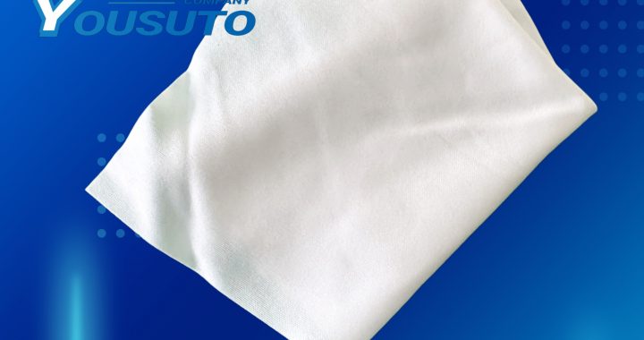
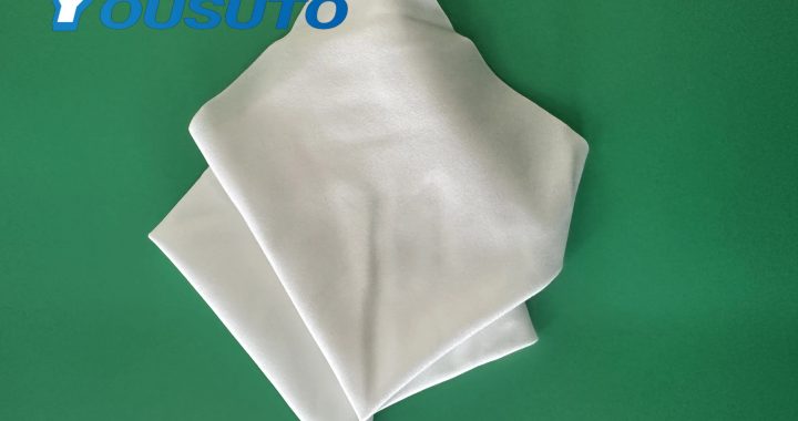
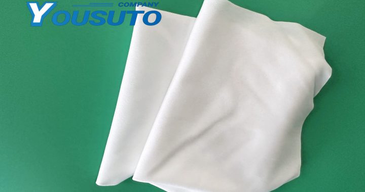
Microfiber prewetted IPA (Isopropyl Alcohol) cleanroom wipes combine high-performance microfiber fabric with 70% IPA solution, making them ideal for industries requiring high cleanliness such as electronics, optics, medical, and cleanroom environments.
1. Material Advantages
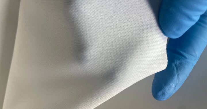
Microfibers have a fine structure with fibers much smaller than regular fibers, offering excellent absorption and particle capture, effectively minimizing fiber shedding and preventing secondary contamination.
2. Prewetted Design
Each wipe is uniformly prewetted with 70% IPA alcohol, ensuring fast and effective removal of oils, fingerprints, and bacteria, improving cleaning and disinfecting efficiency.
3. Application Areas
-
Cleaning electronic screens and components
-
Wiping optical lenses and instruments
-
Disinfecting medical devices and lab equipment
-
Maintaining surfaces in cleanroom environments
4. Usage Tips
Ready to use out of the package without additional alcohol; wipes evaporate quickly after use, leaving no residue or watermarks, maintaining dry, clean surfaces.