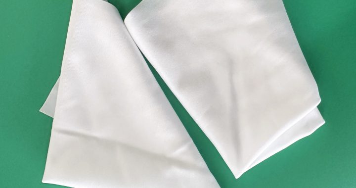
PCB precision equipment—including SMT placement machines, AOI (Automated Optical Inspection) systems, and reflow ovens—relies on ultra-clean, static-free environments to avoid damaging delicate components (e.g., 0.4mm fine-pitch ICs) and ensure accurate manufacturing. Anti-Static cleanroom wipes (static-dissipative or conductive) address two core risks: electrostatic discharge (ESD) that fries microchips, and particulate contamination that causes placement errors or short circuits. Below is their tailored application across key PCB precision equipment cleaning tasks.
1. SMT Placement Machine Cleaning: Protecting Component Pick-and-Place Accuracy
SMT placement machines use tiny nozzles (0.2–0.5mm diameter) to pick and place PCBs’ surface-mount devices (SMDs). Dust buildup on nozzles, feeders, or placement heads causes misalignment, “no-pick” errors, or SMD damage—while ESD can destroy sensitive chips during handling.
- Wipe Selection: Use static-dissipative microfiber wipes (surface resistance: 10⁶–10¹⁰ Ω) for general cleaning; opt for conductive polyester wipes (10³–10⁶ Ω) for nozzle/feeder contacts (high ESD risk). Choose lint-free variants (continuous-filament fibers) to avoid fiber clogging nozzles.
- Application Steps:
- Power down the machine and lock the placement head to prevent movement.
- For nozzles: Fold the wipe into a small pad and gently dab (not rub) nozzle tips—avoids bending delicate nozzle shafts. Use a wipe strip (1mm wide) to clean feeder track grooves (traps dust that jams SMDs).
- For placement heads: Wipe the head’s surface and electrical contacts with a pre-wet anti-static wipe (70% IPA)—removes oil residues from lubricants and dissipates static.
- Outcome: Reduces SMT placement errors by 40–50% and extends nozzle lifespan by 3x (no fiber clogging).
2. AOI System Optical Cleaning: Preserving Inspection Accuracy
AOI systems use high-resolution cameras and lenses to detect PCB defects (e.g., missing solder, misaligned components). Dust on lenses, light sources, or conveyor belts distorts images, leading to false rejects or missed defects—costly in high-volume PCB production.
- Wipe Selection: Choose anti-static optical wipes (deionized water-based or lens-grade IPA) with ultra-fine microfiber (0.1μm diameter) to avoid scratching AR-coated lenses. Ensure wipes meet ISO Class 5 lint standards (≤0.5 fibers per use).
- Application Steps:
- Turn off the AOI’s light source and wait for lenses to cool (prevents thermal shock).
- Use a dry anti-static wipe to gently blot dust from camera lenses—circular motions are prohibited (spread particles); use single linear strokes instead.
- For conveyor belts (hold PCBs during inspection): Wipe the belt’s surface with a pre-wet anti-static wipe (mild surfactant-based) to remove solder balls or flux residue—prevents PCB slippage and inspection misalignment.
- Outcome: Lowers AOI false reject rates from 8% to <1% and eliminates “blind spots” caused by dusty lenses.
3. Reflow Oven Cleaning: Preventing Solder Contamination
Reflow ovens heat PCBs to melt solder paste, but they accumulate solder splatters, flux residues, and dust on heater elements, conveyor rails, and thermal sensors. These contaminants cause uneven heating (leading to cold joints) or conveyor jams—while ESD from standard wipes can damage oven control boards.
- Wipe Selection: Use heat-resistant anti-static wipes (withstands up to 150°C) for post-cooling cleaning; for flux residues, use pre-wet anti-static wipes (99% IPA) that dissolve flux without leaving residues.
- Application Steps:
- Cool the oven to <40°C (critical—hot surfaces evaporate IPA instantly, leaving residues and increasing fire risk).
- Wipe heater elements with a dry anti-static wipe to remove loose solder splatters—use a wipe strip to clean between elements (avoids damaging heating coils).
- For conveyor rails: Wipe the rails and guides with a pre-wet anti-static wipe to remove flux buildup—ensures smooth PCB movement and consistent heating.
- Outcome: Reduces reflow oven-related PCB defects (cold joints, tombstoning) by 35% and extends oven maintenance intervals by 2x.
4. PCB Test Fixture Cleaning: Ensuring Reliable Electrical Contact
Test fixtures (used to validate PCB functionality) have tiny probes (0.1mm diameter) that contact PCB pads. Oxidation, dust, or flux residue on probes causes intermittent connections—leading to false “failed” tests and costly rework. ESD during cleaning can also damage test fixture electronics.
- Wipe Selection: Use anti-static pre-wet wipes (70% IPA) with soft fibers to clean probe tips; for oxidized pads, use conductive anti-static wipes to dissipate static while removing corrosion.
- Application Steps:
- Disconnect the test fixture from power to avoid ESD pathways.
- Gently dab probe tips with a pre-wet wipe—avoid scrubbing (wears down probe plating). Use a wipe strip to clean fixture socket contacts (traps dust that disrupts signal).
- Dry probes immediately with a dry anti-static wipe to prevent moisture-induced oxidation.
- Outcome: Cuts PCB test rework rates by 45% and extends probe lifespan by 50% (no abrasive damage).
Critical Advantages of Anti-Static Wipes for PCB Precision Equipment
- ESD Protection: Prevents static-induced damage to SMDs, test electronics, and machine control boards—avoids losses from ruined components ($0.50–$50 per chip).
- Lint-Free Cleaning: Eliminates fiber contamination that clogs nozzles, distorts AOI images, or causes short circuits.
- Material Compatibility: Safe for PCB materials (FR-4, solder masks, gold-plated pads) and equipment surfaces (aluminum, plastic, optical coatings)—no scratching or degradation.
By integrating anti-static cleanroom wipes into PCB precision equipment cleaning, manufacturers boost production yield, reduce downtime, and protect high-value machinery—critical for meeting the demands of miniaturized, high-density PCBs.
