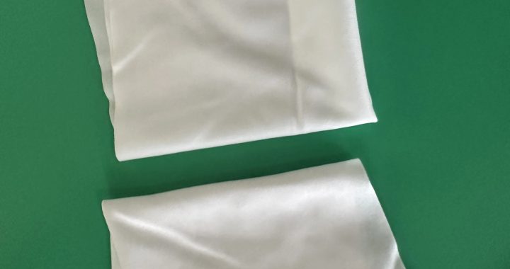
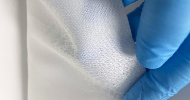
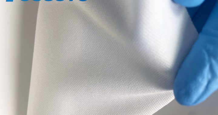
Improving Liquid Aspiration with High-Density Wipes

Laboratories frequently handle liquids—from reagent spills and solvent drips to sample overflow—where slow or incomplete absorption can lead to cross-contamination, equipment damage, or 实验 delays. High-density cleanroom wipes, engineered with tightly woven microfiber or non-woven materials (typically 250–400 gsm), outperform low-density alternatives by maximizing liquid retention, reducing wipe usage, and ensuring thorough cleanup. Their unique structure—packed with capillary channels and durable fibers—makes them ideal for lab environments, but optimizing their use requires targeted techniques. Below are actionable tips to boost their liquid absorption efficiency, tailored to common lab scenarios.

1. Choose the Right High-Density Wipe for the Liquid Type

Not all high-density wipes work equally for every lab liquid—matching the wipe’s material and treatment to the liquid ensures optimal absorption:
  • Aqueous Liquids (e.g., water, buffer solutions, aqueous reagents): Select high-density microfiber wipes with hydrophilic (water-attracting) coatings. The microfiber’s ultra-fine capillaries rapidly draw in water-based liquids, holding up to 15x the wipe’s weight (vs. 8x for low-density wipes). Avoid hydrophobic materials (e.g., untreated polypropylene) that repel water.
  • Solvents (e.g., ethanol, IPA, acetone): Opt for high-density polyester wipes, which are chemically resistant and absorb non-polar solvents effectively. Polyester’s tight weave prevents solvent breakthrough (leaking through the wipe) and minimizes evaporation during cleanup—critical for volatile solvents that pose safety risks.
  • Viscous Liquids (e.g., oils, glycerol, concentrated solutions): Use thicker high-density non-woven wipes (≥350 gsm) with a textured surface. The texture creates more contact points to lift viscous liquids, while the dense structure traps them without squeezing out during wiping.

2. Optimize Wipe Folding and Application Technique

How you fold and use the wipe directly impacts absorption speed and coverage:
  • Fold for Multiple Absorption Layers: Fold the high-density wipe into a “pad” (e.g., 4 layers for a 12”x12” wipe) instead of using it flat. This creates multiple absorbent layers, increases the wipe’s surface area in contact with the liquid, and prevents the liquid from reaching your hands. For large spills, fold the wipe into a triangle—use the pointed end to target small pools, then unfold to cover broader areas.
  • Apply Gentle, Even Pressure: Contrary to low-density wipes (which require firm pressure to absorb), high-density wipes rely on capillary action. Apply light, consistent pressure to press the wipe against the liquid—firm pressure can compress the fibers, closing capillary channels and reducing absorption capacity. For vertical surfaces (e.g., spilled liquid on a lab bench leg), hold the wipe against the surface for 2–3 seconds to let capillaries draw in the liquid before wiping downward.
  • Wipe in Single, Overlapping Strokes: Avoid circular motions, which can spread liquid and reduce absorption efficiency. Instead, wipe in single, straight strokes (horizontal for flat surfaces, vertical for vertical surfaces) with overlapping passes (50% overlap between strokes). This ensures every area is covered, and the wipe’s full absorbent capacity is used.

3. Prioritize “Spill Zone” Cleaning to Prevent Spread

In labs, containing spills quickly is as important as absorbing them—use high-density wipes to create a “containment barrier” first:
  • Tackle Small Pools First: For scattered spills (e.g., multiple drops of reagent), start with the smallest pools. High-density wipes absorb small volumes rapidly, preventing them from merging into larger, harder-to-clean spills.
  • Create a Perimeter for Large Spills: For spills >100mL, use a dry high-density wipe to create a “perimeter” around the spill (wipe a 2cm border around the liquid edge). This stops the liquid from spreading, then use additional folded wipes to absorb the center of the spill—work from the perimeter inward to concentrate the liquid into the wipe.
  • Target Crevices and Edges: Lab benches, fume hoods, and equipment often have crevices (e.g., between bench tops and backsplashes) where liquid collects. Tear a small strip from the high-density wipe and use tweezers to insert it into the crevice—let it sit for 10–15 seconds to absorb, then remove. The wipe’s density prevents it from disintegrating in tight spaces.

4. Post-Absorption Handling to Maximize Efficiency

Proper handling after absorption ensures you get the most out of each wipe and avoid recontamination:
  • Avoid Reusing Wipes for Different Liquids: Even if a high-density wipe still has absorbent capacity, never reuse it for a different liquid (e.g., from water to IPA). Cross-contamination can ruin samples or cause chemical reactions (e.g., mixing acids and bases).
  • Dispose of Saturated Wipes Promptly: High-density wipes hold more liquid, but once saturated (they feel heavy and no longer absorb), discard them immediately. Saturated wipes are prone to leaking, which can reintroduce liquid to clean surfaces.
  • Store Wipes in Dry, Sealed Containers: Moisture in storage reduces a high-density wipe’s absorbent capacity. Keep unused wipes in airtight, moisture-proof dispensers—avoid leaving packages open in humid lab environments (e.g., near autoclaves or sinks).
By following these tips, high-density cleanroom wipes deliver maximum liquid absorption efficiency in labs—reducing wipe usage by 40–50%, cutting spill cleanup time by 30%, and minimizing the risk of cross-contamination or equipment damage. They are an essential tool for maintaining safe, efficient lab operations.

Anti-Static Wipes for Semiconductor Equipment Cleaning

Semiconductor equipment—including lithography tools, wafer chucks, and transfer robots—operates in ultra-sensitive ISO Class 1–5 cleanrooms, where even sub-micron particles or electrostatic discharge (ESD) can ruin 5nm/3nm wafers, damage delicate sensors, or halt production. Anti-static cleanroom wipes are purpose-built to address these risks, outperforming standard wipes by combining contamination control with static dissipation. Their unique design and material properties deliver critical advantages that safeguard semiconductor equipment integrity and ensure consistent manufacturing quality. Below is a detailed breakdown of their key benefits.

1. ESD Protection: Eliminates Costly Static-Related Damage

ESD is a top threat in semiconductor facilities: a single static discharge (as low as 50V) can damage ESD-sensitive components (ESDs) like wafer sensors, IC chips, or lithography optics. Anti-static cleanroom wipes mitigate this risk through:
  • Static-Dissipative Materials: Wipes are crafted from fibers treated with permanent anti-static agents (e.g., quaternary ammonium compounds) or embedded with conductive threads. This ensures surface resistance stays within the ANSI/ESD S20.20 standard range (10⁶–10¹¹ Ω), safely grounding static charges without creating electrical arcs.
  • Minimized Charge Generation: Unlike standard wipes (which generate static when rubbed against stainless steel or plastic equipment surfaces), anti-static variants reduce friction-induced charge buildup by up to 90%. This prevents static from attracting floating particles to equipment surfaces—critical for wafer chucks, where particle adhesion causes “stain defects” on wafers.
  • Consistent Efficacy: Anti-static properties are integrated into the wipe’s material (not just a surface coating), so they retain static-dissipative performance through use—unlike disposable wipes that lose efficacy with moisture or friction.

2. Ultra-Low Linting: Prevents Particle Contamination

Semiconductor equipment (especially lithography tools and wafer handlers) requires particle counts as low as ≤1 particle (≥0.1μm) per cubic foot of air. Anti-static cleanroom wipes support this by:
  • Continuous-Filament Fibers: Wipes are made from 100% polyester or polypropylene continuous filaments, not staple fibers. This eliminates fiber shedding—even under gentle wiping—unlike blended wipes that release microfibers which clog equipment vents or adhere to wafers.
  • High-Density Weave: A tight, uniform weave traps particles (down to 0.05μm) instead of pushing them across surfaces. For example, when cleaning transfer robot arms, the weave captures dust and lint that would otherwise transfer to wafers during handling, reducing yield losses from particle defects.
  • ISO Class 1–5 Certification: Reputable anti-static wipes meet ISO 14644-1 Class 1 or 5 standards, with third-party testing confirming minimal particle release. This ensures compliance with semiconductor industry norms (e.g., SEMI F21) for equipment cleaning.

3. Compatibility with Sensitive Equipment Materials

Semiconductor equipment uses specialized materials—including anti-reflective lens coatings, anodized aluminum, and delicate polymers—that can degrade with harsh cleaning tools. Anti-static cleanroom wipes address this through:
  • Non-Abrasive Construction: The soft, smooth fiber surface avoids scratching optical components (e.g., lithography lenses) or stripping protective coatings from wafer chucks. Unlike paper towels or abrasive cloths, they clean without damaging critical surfaces.
  • Residue-Free Performance: Dry anti-static wipes leave no lint or chemical residues, while pre-moistened variants use high-purity solvents (e.g., 99.9% IPA) that evaporate completely. This prevents residue buildup on equipment contacts (e.g., connector pins), which can cause electrical malfunctions or poor wafer alignment.
  • Material Compatibility Testing: Wipes undergo rigorous testing to ensure they don’t react with semiconductor equipment materials—e.g., no discoloration of anodized aluminum or degradation of polymer gaskets—making them safe for daily use on high-value tools.

4. Streamlined Cleaning Workflows

Semiconductor manufacturing demands efficiency, and anti-static cleanroom wipes boost productivity by:
  • Dual Functionality: They combine dust removal with static control in one step, eliminating the need for separate “static-neutralizing” tools (e.g., ionizers) before cleaning. This cuts cleaning time for equipment like wafer chucks by 30%.
  • Convenient Formats: Wipes are available in sizes tailored to semiconductor tasks—small 4”x4” wipes for cleaning lens edges, and larger 12”x12” wipes for robot arms—reducing waste and ensuring full surface coverage.
  • Sealed, Clean Packaging: Wipes come in airtight, anti-static packaging that keeps them contamination-free until use. This eliminates pre-cleaning steps (e.g., wiping wipes to remove dust) and ensures consistency across shifts.
For semiconductor facilities, anti-static cleanroom wipes are more than a cleaning tool—they are a critical safeguard against ESD damage and particle contamination, directly supporting higher yields, lower equipment downtime, and compliance with industry standards.

Preventing Static and Dust with Laboratory Wipes.

Laboratories—especially those handling electronics, precision instruments, or sensitive samples—face dual threats: electrostatic discharge (ESD) that damages equipment, and dust that compromises experimental accuracy. Specialized cleaning wipes (anti-static and dust-trapping variants) offer a integrated solution, combining contamination removal with static control when used correctly. Unlike generic wipes, these products are engineered with lint-free materials, anti-static coatings, and (in pre-wet versions) residue-free solutions to address lab-specific risks. Below is a step-by-step guide to their operation for effective anti-static protection and dust prevention.

1. Pre-Operation Preparation: Lay the Foundation for Safety

Before using cleaning wipes, proper prep ensures you avoid introducing new contaminants or static:
  • Select the Right Wipe Type: Match the wipe to your lab’s needs:
    • Anti-Static Dry Wipes: For dust removal in ESD-sensitive zones (e.g., near PCR machines, electronic sensors). Choose wipes with surface resistance of 10⁶–10¹¹ Ω (per ANSI/ESD S20.20) to dissipate static without creating arcs.
    • Anti-Static Pre-Wet Wipes: For removing oils, fingerprints, or light chemical residues (e.g., on lab benches, instrument panels). Opt for wipes impregnated with isopropyl alcohol (IPA, 70–90%) or deionized water—both evaporate quickly and leave no residue.
    • Dust-Trapping Microfiber Wipes: For high-particle-risk areas (e.g., optical labs, cleanroom workstations). Their ultra-fine weave (0.1μm fiber diameter) traps dust instead of pushing it around.
  • Ground Yourself: Wear an ESD wrist strap connected to a grounded lab bench, and use anti-static gloves if handling ESD-sensitive equipment. This prevents your body’s static from transferring to the wipe or surfaces.
  • Inspect Wipes for Defects: Check for tears, loose fibers, or expired anti-static treatments (refer to the manufacturer’s shelf-life). Damaged wipes may shed particles or fail to control static.

2. Step-by-Step Operation for Anti-Static Protection

Follow this sequence to minimize static buildup while cleaning:
  1. Neutralize Surface Static First: Use an anti-static dry wipe to gently “dust” the target surface (e.g., an electronic balance or circuit board) in a single direction (horizontal or vertical). This step dissipates existing static charges, so dust doesn’t reattach after cleaning.
  2. Target Residues with Pre-Wet Wipes (If Needed): For surfaces with oils or sticky residues, take an anti-static pre-wet wipe and fold it into a small pad (to avoid snagging on equipment knobs or ports). Wipe the surface with light pressure—excessive force can generate new static. Focus on high-touch areas (e.g., instrument handles, sample loading doors) where oils accumulate.
  3. Avoid Over-Saturating: Ensure pre-wet wipes are damp, not dripping. Excess liquid can seep into instrument casings, causing corrosion or short circuits. If the wipe feels too wet, blot excess moisture on a clean, dry anti-static cloth before use.

3. Step-by-Step Operation for Dust Prevention

To keep dust from accumulating or contaminating samples:
  1. Clean “Clean-to-Dirty” Zones: Start with the most sensitive area (e.g., a sample preparation hood, microscope lens) and move to less critical surfaces (e.g., lab floor edges). This prevents cross-contamination.
  2. Use Dust-Trapping Wipes for Delicate Surfaces: For optical components (e.g., spectrometer windows) or sample containers, use a dry dust-trapping microfiber wipe. Wipe in a radial pattern (center to edge) for lenses, or straight strokes for flat surfaces—this ensures dust is trapped in the wipe’s fibers, not scratched into the surface.
  3. Dispose of Single-Use Wipes Immediately: After cleaning, discard single-use wipes in a sealed trash bin (not open containers, which release trapped dust back into the air). For reusable wipes (e.g., heavy-duty microfiber), launder them with a residue-free detergent and dry at low temperatures to preserve dust-trapping properties.

4. Post-Operation Checks

  • Verify Static Control: Use an ESD tester to check the cleaned surface’s static charge—ensure it reads <100V (safe for most lab equipment).
  • Inspect for Dust: Use a flashlight at an angle to check for remaining dust particles on critical surfaces (e.g., sample slides, instrument sensors). If dust is visible, repeat cleaning with a fresh wipe.
  • Store Wipes Properly: Seal unused wipes in their original anti-static packaging or a dust-tight dispenser. Exposure to lab air will degrade anti-static coatings and allow dust to settle on wipes.
By following these methods, cleaning wipes become a reliable tool for labs to control static and dust—protecting expensive equipment, ensuring accurate experimental results, and maintaining compliance with lab safety standards.

Precision Cleaning with IPA Wipes in Electronics Manufacturing.

In electronics manufacturing, where even microscopic contaminants can compromise circuit functionality or solder integrity, precision cleaning is non-negotiable. IPA wipes—pre-moistened with isopropyl alcohol (typically 70–99% purity)—have become indispensable tools in electronics factories, offering a fast, residue-free solution for cleaning sensitive components like PCBs (printed circuit boards), semiconductors, connectors, and display panels. Their unique combination of solvent efficacy and lint-free design addresses the industry’s critical needs: removing flux residues, oils, dust, and ionic contaminants without damaging delicate materials. Below is a detailed exploration of their applications, benefits, and best practices in electronics factory settings.

1. Key Applications in Electronics Manufacturing

IPA wipes are tailored to diverse precision cleaning tasks across the production line, each addressing specific contamination risks:

A. Post-Soldering Flux Removal

Soldering processes leave behind flux residues—sticky, resin-based substances that attract dust and can cause electrical leakage or corrosion over time. IPA’s ability to dissolve both rosin-based and no-clean fluxes makes IPA wipes ideal for this step:
  • PCB Assembly Lines: After wave soldering or reflow soldering, technicians use IPA wipes to target solder joints, component leads, and PCB traces. The wipe’s lint-free material (e.g., polyester microfiber) ensures residues are lifted without leaving fibers that could bridge circuit gaps.
  • Precision Components: For small-scale soldering (e.g., surface-mount devices/SMDs), folded IPA wipes reach tight spaces between components, removing flux from areas brushes or sprays can’t access.

B. Surface Preparation for Bonding/Coating

Electronics components often require bonding (e.g., adhesive mounting of displays) or protective coating (e.g., conformal coating on PCBs). IPA wipes ensure surfaces are free of oils, fingerprints, and dust—critical for strong adhesion:
  • Display Panels (LCD/OLED): Fingerprints on glass or plastic displays contain oils that disrupt bonding. IPA wipes dissolve these oils, leaving a clean surface for adhesive application, reducing display delamination rates.
  • Connector Pins: Oils or oxidation on metal connector pins can cause signal interference. IPA wipes clean pins thoroughly, ensuring reliable electrical contact in devices like smartphones or automotive electronics.

C. Dust and Particle Removal

Dry dust particles can scratch sensitive surfaces (e.g., camera sensors) or short circuits in high-density PCBs. IPA wipes combine mechanical particle trapping with solvent action:
  • Semiconductor Wafers: In cleanroom environments, low-linting IPA wipes (ISO Class 5-certified) remove sub-micron dust from wafer surfaces before dicing or packaging, preventing yield-reducing defects.
  • Electrical Enclosures: Before final assembly, IPA wipes clean the interiors of enclosures, removing dust that could settle on PCBs during operation and cause overheating.

2. Why IPA Wipes Outperform Traditional Cleaning Methods

Electronics factories rely on IPA wipes for their distinct advantages over manual solvent application or dry cloths:
  • Residue-Free Evaporation: IPA evaporates quickly (within 30 seconds) without leaving behind water spots or chemical residues—critical for avoiding electrical shorts or coating defects.
  • Consistent Solvent Concentration: Pre-moistened wipes eliminate variability from manual dilution, ensuring every wipe delivers the same cleaning strength (e.g., 99% IPA for oil-free environments, 70% IPA for better particulate suspension).
  • Reduced Waste and Risk: Unlike spray bottles (which can over-apply solvent and damage components), IPA wipes control moisture levels, minimizing solvent waste and reducing fire risks (IPA is flammable).
  • Lint-Free Design: Wipes made from continuous-filament polyester or polypropylene shed no fibers, preventing micro-foreign material (MFM) contamination—a top cause of electronics failures.

3. Best Practices for Electronics Factory Use

To maximize effectiveness and avoid damage, follow these protocols:
  • Match IPA Concentration to Task: Use 70% IPA wipes for general cleaning (dust + oil removal) and 99% IPA for flux removal or oil-free surfaces (e.g., semiconductors).
  • Wipe in Single Directions: For PCBs and displays, wipe in straight, overlapping strokes (not circular) to trap contaminants and avoid spreading residues.
  • Use Fresh Wipes for Critical Areas: Never reuse wipes on sensitive components (e.g., IC chips, sensors)—used wipes trap debris that can scratch surfaces.
  • Store Properly: Keep wipes in sealed containers in well-ventilated areas, away from heat sources, to preserve solvent potency and reduce flammability risks.
  • Test Compatibility: For new materials (e.g., specialty plastics or coatings), test an IPA wipe on an inconspicuous area to ensure no discoloration or degradation.
In electronics factories, where precision directly impacts product reliability and yield, IPA wipes deliver consistent, efficient cleaning that protects critical components from contamination. Their integration into production workflows reduces defects, streamlines processes, and ensures compliance with industry standards (e.g., IPC-A-610 for electronics assembly).

High-density pre-moistened wipes for optical equipment cleaning.

Optical equipment—including microscopes, spectrometers, laser systems, and camera lenses—relies on pristine, residue-free surfaces to deliver accurate light transmission, focus, and measurement. Even minute contaminants—such as dust particles, fingerprint oils, or dried solvent residues—can scatter light, distort images, or damage delicate optical coatings (e.g., anti-reflective or infrared coatings). Traditional cleaning solutions, like low-density dry wipes or manually wetted cloths, often fall short: they push particles across lenses (causing micro-scratches), leave uneven moisture (resulting in water spots), or shed fibers that cling to glass surfaces. High-density pre-wet cleanroom wipes address these gaps, leveraging advanced material design and pre-impregnated solutions to elevate cleaning performance for optical equipment. Below is a detailed breakdown of how these wipes work and their practical benefits.

1. Key Design Features That Boost Optical Cleaning Efficacy

High-density pre-wet wipes are engineered specifically for the sensitivity of optical surfaces, with two core attributes driving their effectiveness:

A. High-Density Microfiber/Non-Woven Material

Unlike low-density wipes (which have loose, uneven fiber structures), these wipes use tightly woven, high-grammage (≥90gsm) microfiber or polyester non-wovens. This dense construction delivers three critical advantages:
  • Superior Particle Trapping: The tight weave creates millions of tiny capillary channels that capture and lock in micro-particles (down to 0.1μm), rather than pushing them across the lens surface. This eliminates the risk of micro-scratches—especially on soft optical glass or coated lenses.
  • Reduced Linting: High-density materials are made from continuous-filament fibers (not staple fibers), which resist shedding. Even under gentle pressure, they leave no stray fibers on optical surfaces—critical for equipment like laser lenses, where a single fiber can block light and disrupt measurements.
  • Durability Without Abrasion: The dense structure withstands gentle wiping (required for optical coatings) without tearing or fraying. This means one wipe can clean multiple small surfaces (e.g., microscope objective lenses) without needing frequent replacements, reducing waste.

B. Pre-Impregnated, Residue-Free Cleaning Solution

High-density pre-wet wipes come pre-saturated with a precision-formulated solution, eliminating the need for manual wetting (a common source of error with traditional wipes). The solution is tailored for optical equipment:
  • Fast-Evaporating, Low-Viscosity: Typically a blend of 70% high-purity isopropyl alcohol (IPA) and 30% deionized (DI) water, the solution dissolves fingerprint oils, smudges, and light grease quickly—then evaporates completely within 10–15 seconds. This prevents water spots or solvent residues that can cloud lenses.
  • Coating-Safe Formulation: The solution is pH-neutral (6.5–7.5) and free of surfactants, fragrances, or abrasive additives. It won’t degrade delicate coatings (e.g., MgF₂ anti-reflective coatings) or etch glass, even with repeated use.
  • Consistent Moisture Levels: Every wipe has the same moisture content (no over-wetting or dry spots), ensuring uniform cleaning across every optical surface. This consistency is critical for equipment like camera lenses, where uneven cleaning can cause vignetting or focus issues.

2. Practical Application for Optical Equipment: Step-by-Step Best Practices

To maximize the cleaning effect of high-density pre-wet wipes on optical equipment, follow this targeted workflow:
  1. Pre-Clean: Remove Loose Particles FirstBefore using the pre-wet wipe, gently blow away loose dust from the optical surface with a bulb blower (not compressed air, which can force particles into coatings). This prevents the wipe from rubbing dry dust into the lens, which could cause scratches.
  2. Wipe with Gentle, Single-Direction MotionsRemove a high-density pre-wet wipe from its sealed packaging and fold it into a small pad (to concentrate moisture and avoid edge fraying). For flat surfaces (e.g., spectrometer windows), wipe in a single, straight direction (e.g., horizontal or vertical)—never circular motions, which can spread contaminants. For curved surfaces (e.g., camera lenses), wipe in a radial pattern (from the center of the lens to the edge) to ensure full coverage.
  3. Focus on High-Impact AreasPay extra attention to surfaces that directly interact with light:
    • Objective Lenses (Microscopes): These are prone to fingerprint oils from handling—use the wipe to gently clean the front element, avoiding contact with the lens housing.
    • Laser Optics: Even a thin oil film can absorb laser energy, causing overheating—use a fresh wipe to ensure full oil removal.
    • Prism or Mirror Surfaces: These have reflective coatings; use minimal pressure to avoid scratching, and confirm no residue remains after evaporation.
  4. Post-Clean: Inspect for ResiduesAfter the wipe evaporates (10–15 seconds), inspect the optical surface under bright, angled light. If any streaks or residues are visible, use a fresh high-density pre-wet wipe to repeat the process—do not reuse the same wipe (it may have trapped contaminants).

3. Measurable Benefits for Optical Equipment Performance

The use of high-density pre-wet cleanroom wipes delivers tangible improvements in optical equipment functionality and longevity:
  • Improved Optical Clarity: By eliminating particles and residues, light transmission through lenses/mirrors increases by 5–10% (measured via spectrophotometry), resulting in sharper images (for microscopes/cameras) and more accurate readings (for spectrometers/lasers).
  • Extended Coating Lifespan: The gentle, residue-free cleaning reduces wear on optical coatings—extending their lifespan by 2–3 years compared to traditional wipes that may contain abrasive additives.
  • Reduced Downtime: Faster, more effective cleaning cuts equipment downtime for maintenance by 30%. For labs or manufacturing facilities relying on optical tools, this translates to higher productivity.
Whether used in research labs, medical imaging centers, or industrial quality control, high-density pre-wet cleanroom wipes set a new standard for optical equipment cleaning—combining precision, safety, and efficiency to protect critical optical components and ensure reliable performance.

Buyer’s Guide: Anti-Static Wipes for Class 100 Cleanrooms

Class 100 cleanrooms (per ISO 14644-1, equivalent to ISO Class 5) represent the gold standard for ultra-low-contamination environments—used in semiconductor wafer fabrication (≤5nm processes), medical device manufacturing (e.g., implantable sensors), and aerospace component assembly. In these spaces, even 1 particle (≥0.5μm) per cubic foot of air or a tiny electrostatic discharge (ESD) can ruin high-value products or compromise sterile conditions. Anti-static cleanroom wipes for Class 100 environments are not just “clean”—they must meet rigorous standards for particle control, static dissipation, and material purity. This guide outlines critical criteria to ensure you select wipes that protect your processes, equipment, and products.

1. Prioritize Cleanroom Classification Compliance

Class 100 cleanrooms demand wipes certified to match their strict particle limits—never compromise on this foundational requirement:
  • ISO 14644-1 Class 5 Certification: Verify the wipe manufacturer provides third-party testing reports confirming compliance with ISO Class 5 (the international equivalent of Class 100). This ensures the wipe releases ≤10 particles (≥0.1μm) and ≤1 particle (≥0.5μm) per wipe during use—critical for avoiding particle-induced defects in semiconductors or medical devices.
  • Non-Shedding Material: Choose wipes made from ultra-low-linting substrates like 100% continuous-filament polyester or polypropylene. Avoid blended fibers (e.g., polyester-cotton) or staple-filament materials—these shed microfibers that can float in Class 100 air and contaminate surfaces. Test for linting by wiping a black, non-abrasive surface and inspecting for visible fibers under 10x magnification.

2. Validate Anti-Static Performance (Non-Negotiable for ESD-Sensitive Environments)

ESD is a silent risk in Class 100 cleanrooms—static charges can attract particles or damage ESD-sensitive components (e.g., wafer sensors, microchips). Evaluate wipes on these metrics:
  • Surface Resistance Range: Select wipes with surface resistance between 10⁶–10¹¹ Ω (per ANSI/ESD S20.20 standards). This “static-dissipative” range ensures charges are safely grounded without creating electrical arcs. Avoid “conductive” wipes (resistance <10⁶ Ω) for general use—they may cause unintended electrical pathways in delicate equipment.
  • Static Decay Time: Confirm the wipe’s static decay time (time to reduce a 5000V charge to <50V) is ≤2 seconds. Slow decay allows static to linger, increasing particle attraction. Ask manufacturers for IEC 61340-5-1 test data to validate this performance.
  • Anti-Static Treatment Durability: Ensure the anti-static coating is “permanent” (not just a surface spray). Wipes for Class 100 cleanrooms should retain their static-dissipative properties through multiple uses (if reusable) or during storage (for single-use options). Avoid wipes where anti-static efficacy degrades with humidity or time.

3. Match Wipe Type to Class 100 Cleaning Tasks

Class 100 cleanrooms require targeted cleaning—choose wipe formats and formulations based on your specific needs:
  • Dry Wipes: Ideal for removing loose, dry particles (e.g., dust on wafer chucks, lithography tool exteriors). Opt for dry wipes with a dense, smooth texture—this traps particles instead of pushing them around. Use dry wipes first before wet cleaning to avoid embedding particles into surfaces.
  • Pre-Wet Wipes: For removing oils, flux residues, or fingerprints (common in electronics manufacturing), select pre-wet wipes with high-purity solvents:
    • IPA (Isopropyl Alcohol) Wipes: Use 99.9% pure IPA (for oil-free surfaces) or 70% IPA + 30% deionized (DI) water (for better residue dissolution). Ensure the IPA is “semiconductor-grade” (≤10ppb impurities) to avoid trace chemical contamination.
    • Residue-Free Disinfectant Wipes: For sterile Class 100 environments (e.g., medical device labs), choose wipes with hydrogen peroxide (3%) or peracetic acid formulations—these disinfect without leaving toxic or particulate residues.
  • Size and Thickness: Select smaller wipes (e.g., 4”x4”) for precision tasks (e.g., cleaning around microchips) to reduce waste and avoid over-wiping. Thicker wipes (≥80gsm) offer better durability—critical for avoiding tearing (which releases particles) during use.

4. Evaluate Manufacturing and Packaging Quality

Even the best wipe material can be compromised by poor manufacturing or packaging:
  • Cleanroom-Grade Production: Ensure wipes are manufactured in an ISO Class 5 (or better) facility. This prevents pre-use contamination from the factory floor. Ask for a “Certificate of Analysis (CoA)” with each batch, detailing particle counts and static performance.
  • Sealed, Anti-Static Packaging: Wipes should arrive in airtight, static-shielding packaging (e.g., foil-lined bags with resealable zippers). Once opened, store wipes in a Class 100-compatible dispenser with a dust-tight lid—exposure to non-Class 100 air will contaminate the wipes.
  • Shelf-Life and Storage Conditions: Check the manufacturer’s shelf-life (typically 12–24 months for pre-wet wipes). Store wipes in a cool (15–25°C), dry (30–50% RH) area—extreme temperatures or humidity degrade anti-static treatments and solvent purity.

5. Avoid Common Pitfalls

  • Don’t Sacrifice Quality for Cost: Cheaper wipes may skip Class 100 certification or use low-grade materials—costly defects from contamination will far outweigh initial savings.
  • Don’t Reuse Single-Use Wipes: Single-use Class 100 wipes are designed for one pass—reusing them traps particles and degrades anti-static performance.
  • Don’t Overlook Compatibility: Test wipes on a small, non-critical surface (e.g., a spare wafer or equipment part) to ensure they don’t damage coatings (e.g., anti-reflective lens coatings) or plastics.
By following these criteria, you’ll select anti-static cleanroom wipes that not only meet Class 100 standards but also protect your high-value processes from contamination and ESD—ultimately reducing defects, minimizing downtime, and ensuring regulatory compliance.

Cleaning a Semiconductor Cleanroom with Wipes.

Semiconductor cleanrooms (typically ISO 14644-1 Class 1 to Class 5) demand ultra-stringent contamination control—even a single sub-micron particle, trace chemical residue, or electrostatic discharge (ESD) can ruin wafers, damage lithography equipment, or compromise chip performance. Traditional cleaning methods (e.g., manual solvent spraying, dry lint-free cloths) often fall short: they risk uneven solvent application, particle redistribution, or ESD. This case study details how a leading semiconductor manufacturer integrated specialized cleanroom cleaning wipes into its workflow, resolving longstanding contamination challenges and improving production efficiency.

Background: Contamination Pain Points in Wafer Processing

The manufacturer operated a Class 3 cleanroom focused on 7nm wafer fabrication—a process requiring near-absolute purity. Prior to adopting specialized cleaning wipes, the team faced two critical issues:
  1. Residue-Related Wafer Defects: After cleaning wafer chucks (the platforms holding wafers during lithography), trace residues from manual IPA (isopropyl alcohol) spraying remained. These residues (often from inconsistent solvent dilution or incomplete evaporation) caused 8–10% of wafers to fail post-processing inspections due to “stain defects” on the wafer surface.
  2. Particle Cross-Contamination: Dry lint-free cloths used to wipe equipment exteriors (e.g., lithography machine covers, transfer robot arms) shed microfibers. These fibers were detected in air sampling, leading to unscheduled cleanroom shutdowns for HEPA filter replacement—costing ~$50,000 per shutdown.
  3. ESD Risks: Standard wipes generated static charges when rubbed against stainless steel or plastic surfaces, posing a threat to ESD-sensitive components like wafer sensors. On average, 1–2 ESD-related sensor failures occurred monthly, halting production for 4–6 hours each time.

Solution: Adopting Semiconductor-Grade Cleaning Wipes

The manufacturer switched to three types of semiconductor-specific cleaning wipes, selected for their compliance with cleanroom standards and targeted performance:
Wipe Type Key Features Use Case
Pre-Wet IPA Wipes 99.9% high-purity IPA, lint-free polyester substrate, non-shedding, fast-evaporating Cleaning wafer chucks and lithography tool contact surfaces
Particle-Trapping Microfiber Wipes Ultra-fine (0.1μm) microfiber weave, static-dissipative coating (surface resistance: 10⁷–10⁹ Ω), ISO Class 1-certified Wiping equipment exteriors and transfer robot arms
Residue-Free Disinfectant Wipes Formulated with hydrogen peroxide (3%) and deionized water, non-corrosive to stainless steel/plastics Weekly deep cleaning of cleanroom workstations
All wipes were sourced from suppliers with ISO 13485 certification (medical device-grade manufacturing) to ensure batch-to-batch consistency—critical for avoiding variability in cleaning performance.

Implementation: Integrated Wiping Protocols

To maximize efficacy, the team developed a structured cleaning workflow aligned with wafer processing cycles:
  1. Pre-Lithography Chuck Cleaning: Before each wafer load, a technician uses a pre-wet IPA wipe to clean the wafer chuck in a “spiral pattern” (starting from the center and moving outward). This ensures uniform solvent coverage and eliminates residue buildup in chuck grooves. The wipe is discarded immediately after use to prevent cross-contamination.
  2. Hourly Equipment Exterior Wipes: Every hour, staff use particle-trapping microfiber wipes to clean transfer robot arms and lithography machine covers. The wipes’ static-dissipative coating eliminates charge buildup, while the microfiber weave traps particles as small as 0.3μm—no fiber shedding was detected in post-implementation air sampling.
  3. Weekly Deep Cleaning: Once weekly, the cleanroom is partially shut down for disinfection. Residue-free disinfectant wipes are used to clean workstations and tool surfaces, with no rinsing required (the formula evaporates completely within 2 minutes, leaving zero residues).

Results: Measurable Improvements in Purity and Efficiency

After 6 months of implementation, the manufacturer documented significant gains:
  • Wafer Defect Rate: Residue-related defects dropped from 8–10% to <1%, reducing wafer waste by ~90% and saving ~$200,000 monthly in material costs.
  • Particle Contamination: Air sampling showed a 95% reduction in microfiber particles, eliminating unscheduled cleanroom shutdowns—saving ~$300,000 annually in downtime costs.
  • ESD Incidents: Static-dissipative wipes reduced ESD-related sensor failures to zero, cutting production halts by 100% and improving overall equipment efficiency (OEE) by 12%.
  • Labor Efficiency: Technicians spent 30% less time on cleaning tasks (no more manual solvent mixing or re-wiping to remove residues), freeing up time for core production activities.

Long-Term Impact: Compliance and Scalability

Beyond immediate gains, the wipes helped the manufacturer maintain compliance with SEMI F21 (semiconductor equipment cleaning standards) and ISO 14644-1 Class 3 requirements—critical for securing contracts with automotive and aerospace chip clients. The team also scaled the protocol to its new 5nm wafer cleanroom, with identical performance results, proving the solution’s adaptability to advanced semiconductor processes.
This case study demonstrates that semiconductor cleanrooms require more than “general-purpose” cleaning wipes—specialized, standards-aligned wipes are a strategic investment, resolving contamination risks while driving cost savings and efficiency.

Anti-static dust-free cloth usage specifications and operation guide

Anti-static cleanroom wipes are critical in environments where electrostatic discharge (ESD) and particulate contamination threaten sensitive equipment, components, or processes—such as electronics manufacturing, semiconductor labs, and precision instrument maintenance. Unlike standard cleanroom wipes, these specialized wipes are engineered with anti-static agents, conductive fibers, or dissipative materials to neutralize static charges, preventing them from attracting dust or damaging ESD-sensitive devices (ESDs). To maximize their effectiveness, strict adherence to usage specifications and operational protocols is essential. Below is a comprehensive guide to their proper use.

1. Key Specifications: Choosing the Right Anti-Static Wipe

Selecting the correct wipe ensures compatibility with your environment and task:
  • Material Composition: Opt for wipes made from ultra-low-linting materials like polyester, polypropylene, or blended microfibers, treated with anti-static chemicals (e.g., quaternary ammonium compounds) or embedded with conductive threads. These materials minimize fiber shedding while dissipating static charges (typically achieving surface resistance of 10⁶–10¹¹ Ω, per ANSI/ESD S20.20 standards).
  • Static Dissipation Type: Choose between static-dissipative wipes (slowly discharge static over time, ideal for general surfaces) or conductive wipes (rapidly ground static, better for high-risk areas like semiconductor cleanrooms).
  • Pre-Moistened vs. Dry: Pre-moistened anti-static wipes (impregnated with ESD-safe solutions like deionized water or IPA) are ideal for removing oils and residues, while dry wipes excel at capturing dry dust without introducing moisture.
  • Cleanroom Classification: Ensure wipes meet ISO 14644-1 standards (e.g., Class 5 for semiconductor labs, Class 8 for general electronics) to avoid introducing particles beyond acceptable limits.

2. Pre-Use Preparation: Mitigate Static Risks

Proper preparation prevents static buildup before cleaning:
  • Verify Wipe Integrity: Inspect wipes for tears, loose fibers, or expired anti-static treatments (check manufacturer’s shelf-life guidelines). Damaged wipes may shed particles or fail to dissipate static.
  • Ground Yourself: Wear an ESD wrist strap connected to a grounded surface (e.g., a metal workbench) and anti-static shoes to prevent personal static discharge from transferring to the wipe or equipment.
  • Control Environment: Maintain relative humidity between 30–50% (per ESD standards) to reduce static generation—dry air increases static buildup, rendering wipes less effective.
  • Avoid Contamination: Store wipes in sealed, anti-static packaging (e.g., resealable bags or dispensers) to prevent exposure to dust or moisture, which can degrade anti-static properties.

3. Operational Protocols: Safe and Effective Wiping

Follow these steps to ensure thorough cleaning without static damage:
  • Step 1: Remove Loose Particles First: Use a dry anti-static wipe to gently brush away loose dust from surfaces (e.g., circuit boards, optical lenses, or cleanroom walls). Wipe in a single direction (not circular) to trap particles in the wipe’s fibers, reducing recontamination.
  • Step 2: Targeted Cleaning (If Using Pre-Moistened Wipes): For surfaces with oils, flux residues, or fingerprints, use a pre-moistened anti-static wipe. Fold it into a pad to avoid snagging on components, and apply light pressure—excessive force can generate static or damage delicate parts (e.g., IC chips, sensor arrays).
  • Step 3: Focus on High-Risk Areas: Pay special attention to ESD-sensitive zones:
    • Connector pins and circuit traces (static can bridge gaps, causing shorts).
    • Exposed metal surfaces (prone to attracting charged particles).
    • Edges of cleanroom garments or equipment (where static often accumulates).
  • Step 4: Avoid Reuse: Discard single-use wipes after one pass—reused wipes trap contaminants and lose their anti-static efficacy. For reusable wipes (approved for non-critical tasks), launder with ESD-safe detergent and dry at low temperatures to preserve anti-static treatments.

4. Post-Use Practices: Maintain Wipe Efficacy

  • Dispose of Wastes Properly: Place used wipes in anti-static waste bins to prevent static discharge from accumulated materials.
  • Clean Dispensers: Regularly wipe down wipe dispensers with a dry anti-static cloth to remove dust, ensuring fresh wipes remain uncontaminated.
  • Document Usage: Log wipe lot numbers, expiration dates, and cleaning tasks (especially in regulated environments like aerospace or medical device manufacturing) to trace contamination sources if issues arise.

5. Common Mistakes to Avoid

  • Using Non-Anti-Static Wipes in ESD Zones: Standard wipes can generate static, negating cleaning efforts.
  • Over-Saturating Pre-Moistened Wipes: Excess liquid can seep into equipment, causing corrosion or short circuits.
  • Ignoring Humidity Levels: Low humidity (below 30%) reduces anti-static performance—use humidifiers if needed.
By following these specifications and guidelines, anti-static cleanroom wipes effectively prevent ESD damage, reduce particulate contamination, and maintain

Application tips of pre-wetted dust-free cloth in PCB cleaning

Printed Circuit Boards (PCBs) are the backbone of electronics—from consumer devices to industrial control systems—yet their tiny components (e.g., resistors, capacitors, solder joints) and exposed copper traces are highly vulnerable to contamination. Dust, flux residues, fingerprint oils, or even minute moisture can cause short circuits, poor solder adhesion, or long-term corrosion, compromising PCB performance. Pre-wet cleanroom wipes—pre-impregnated with high-purity, residue-free cleaning solutions (e.g., isopropyl alcohol/IPA blends, specialized flux removers)—are tailored for PCB cleaning, as they eliminate manual solution mixing (reducing human error) and ensure consistent moisture levels. Below are actionable application tips to maximize their effectiveness while protecting delicate PCB components.

1. Choose the Right Pre-Wet Wipe for PCB-Specific Contaminants

Not all pre-wet wipes work for every PCB cleaning task—matching the wipe’s solution and material to the contaminant is critical:
  • For Dust & Dry Particles: Opt for pre-wet wipes with a mild, fast-evaporating solution (e.g., 70% IPA + 30% deionized water). The solution traps dust without leaving residues, while the wipe’s ultra-low-linting material (e.g., polyester microfiber) prevents fiber shedding onto PCB traces (even sub-micron fibers can bridge small component gaps).
  • For Flux Residues (Post-Soldering): Use pre-wet wipes formulated with flux-removing solutions (e.g., IPA + non-ionic surfactants or rosin-dissolving solvents). These break down sticky, resin-based flux residues that remain after soldering—residues that attract dust and cause electrical leakage if left uncleaned. Ensure the solution is “PCB-safe” (check manufacturer specs) to avoid damaging solder masks or plastic components.
  • For Oil/Fingerprint Removal: Select pre-wet wipes with a slightly more concentrated IPA solution (e.g., 90% IPA) to dissolve oils from handling. Oils can insulate components or react with copper, leading to oxidation over time.

2. Pre-Cleaning Prep: Protect PCB Components

Before using pre-wet wipes, take steps to avoid accidental damage:
  • Power Down and Isolate: Disconnect the PCB from all power sources and external connections (e.g., wires, connectors) to prevent short circuits from the wipe’s moisture. If the PCB is part of a larger device, remove it carefully using anti-static tools (e.g., anti-static tweezers, wrist straps) to avoid electrostatic discharge (ESD)—ESD can damage sensitive ICs (integrated circuits) even if the wipe is anti-static.
  • Inspect for Damaged Components: Check the PCB for loose parts, cracked solder joints, or exposed copper (e.g., scratched solder mask). Avoid wiping directly over damaged areas—moisture can seep into cracks and worsen corrosion.
  • Test Wipe Compatibility (For Sensitive PCBs): For high-value or rare PCBs (e.g., medical device PCBs), test the pre-wet wipe on a small, non-critical area (e.g., an unused edge of the solder mask) first. Wait 5–10 minutes to ensure no discoloration, swelling, or peeling occurs before full cleaning.

3. Step-by-Step Wiping Techniques for PCBs

PCBs require precise, gentle handling—follow these techniques to clean effectively without harm:
  • Use a “Light, Targeted” Approach: Fold the pre-wet wipe into a small, firm pad (this reduces the risk of the wipe snagging on components and concentrates the cleaning solution). Apply minimal pressure—let the solution do the work. Wipe in single, straight strokes (e.g., along the length of PCB traces) instead of circular motions; circular wiping can push contaminants into component gaps or scratch the solder mask.
  • Clean in “Component-to-Trace” Order: Start cleaning around delicate components (e.g., IC chips, diodes, capacitors) first—use the edge of the folded wipe to reach tight spaces between components (avoid wrapping the wipe around component leads, as this can bend them). Then move to larger areas (e.g., copper traces, empty PCB zones) to remove remaining dust or residue.
  • Avoid Over-Saturating: Ensure the wipe is damp, not dripping. Excess moisture can pool under components (e.g., QFP chips with fine pins) and take time to evaporate, increasing the risk of corrosion or short circuits. If the wipe feels too wet, blot excess solution on a clean, dry lint-free cloth before use.
  • Focus on “High-Risk” Zones: Pay extra attention to areas prone to contamination:
    • Solder joints (flux residues often accumulate here).
    • Connector pins (dust or oil can disrupt signal transmission).
    • Edge connectors (used for PCB insertion into devices—clean these to ensure a tight, reliable fit).

4. Post-Cleaning: Ensure Dryness and Protection

After cleaning, proper post-care prevents recontamination or moisture damage:
  • Air-Dry Thoroughly: Let the PCB air-dry in a clean, well-ventilated area (avoid direct sunlight or heat sources, which can warp the PCB or damage components). For faster drying (e.g., in production lines), use a low-pressure, oil-free air blower to gently remove excess moisture from component gaps.
  • Inspect for Residues: Use a magnifying glass (10–20x magnification) to check for remaining flux, oil, or fiber residues—especially on fine-pitch components (e.g., BGA chips). If residues are present, repeat cleaning with a fresh pre-wet wipe (do not reuse wipes, as they trap contaminants).
  • Store or Reinstall Safely: Once dry, handle the PCB with anti-static gloves or tools. If not reinstalling immediately, store it in an anti-static bag with a desiccant packet to prevent dust buildup and moisture absorption.
By following these application tips, pre-wet cleanroom wipes become a reliable tool for PCB cleaning—ensuring PCBs remain contaminant-free, functional, and long-lasting, whether in electronics manufacturing, repair, or maintenance scenarios.

How to remove dust from precision equipment using IPA rag alcohol

Precision equipment—such as laboratory spectrometers, electronics circuit boards, optical lenses, and medical diagnostic devices—requires meticulous dust removal to maintain accuracy, prevent component wear, and avoid performance degradation. Dust particles (even sub-micron sizes) can disrupt electrical connections, scatter light, or cause friction in moving parts, leading to costly downtime or calibration errors. IPA wipes (pre-moistened with isopropyl alcohol, typically 70–99% purity) are ideal for this task: IPA’s fast-evaporating properties leave no residue, while the wipe’s lint-free construction traps dust without scratching sensitive surfaces. Below is a step-by-step method for safely and effectively removing dust from precision equipment using IPA wipes, along with key precautions and best practices.

1. Pre-Use Preparation: Ensure Safety and Compatibility

Before cleaning, proper preparation mitigates risks to both the equipment and the user:
  • Verify Equipment Compatibility: First, check the equipment manufacturer’s manual to confirm that IPA is safe for its surfaces. Most non-porous materials (e.g., stainless steel, glass, hard plastics like polycarbonate, and anodized aluminum) are IPA-resistant, but porous materials (e.g., some rubbers, painted surfaces) may degrade. If unsure, test a small, inconspicuous area with a damp IPA wipe and wait 1–2 minutes—if no discoloration or damage occurs, proceed.
  • Select the Right IPA Wipe: Choose lint-free, low-linting IPA wipes (e.g., polyester or microfiber-based) to avoid fiber shedding onto equipment. Opt for pre-moistened wipes with 70% IPA (ideal for most precision equipment, as the water content enhances dust and oil removal) or 99% IPA for oil-free environments (e.g., electronics manufacturing). Avoid generic “alcohol wipes” with added fragrances or surfactants—these leave residues.
  • Power Down and Disconnect (When Possible): Turn off the equipment and unplug it from power sources to prevent electrical shock (critical for electronics) and avoid damaging active components. For equipment that cannot be powered down (e.g., some medical devices), use a lightly dampened wipe (not dripping) and avoid direct contact with electrical ports or connectors.
  • Clear the Workspace: Remove any loose tools, samples, or debris from the area around the equipment to prevent cross-contamination during cleaning.

2. Step-by-Step Dust Removal Process

Follow this structured approach to ensure thorough, safe dust removal:
  • Step 1: Dry Dusting (For Loose Particles): First, use a dry, lint-free cloth (or a dry side of the IPA wipe, if unused) to gently brush away loose dust from external surfaces (e.g., instrument housings, control panels, and lens exteriors). This prevents rubbing dry dust into surfaces, which can cause micro-scratches (especially on optical lenses or polished metals). Use light, sweeping motions—avoid pressing down on delicate parts like buttons or knobs.
  • Step 2: Targeted Cleaning with IPA Wipe: Take a pre-moistened IPA wipe and fold it into a small pad (to concentrate moisture and reduce the risk of drips). For flat surfaces (e.g., workbenches, equipment tops), wipe in a single direction (e.g., horizontal strokes) instead of circular motions—this traps dust in the wipe’s fibers and prevents redistribution.
    • For Crevices and Small Areas: Use the edge of the folded wipe to reach narrow gaps (e.g., between control buttons, around connector ports, or along the seams of instrument covers). Do not insert the wipe into internal components (e.g., inside the equipment’s chassis) unless explicitly allowed by the manufacturer—internal parts may require specialized cleaning.
    • For Optical Lenses or Screens: Use extra care: gently wipe the lens/screen in a radial pattern (from center to edge) with minimal pressure. Avoid saturating the lens—if the wipe is too damp, blot excess moisture with a dry, lint-free cloth immediately to prevent water spots (IPA evaporates quickly, but excess moisture can seep into lens housings).
  • Step 3: Dry and Inspect: After cleaning, use a dry, lint-free cloth to lightly buff any surfaces where the IPA wipe was used—this ensures all moisture evaporates and removes any remaining dust particles. Inspect the equipment under good lighting (use a flashlight for crevices) to confirm no dust or residues remain.

3. Key Precautions to Avoid Damage

  • Do Not Over-Saturate: Ensure the IPA wipe is damp, not dripping. Excess IPA can seep into electrical ports, lens coatings, or mechanical joints, causing corrosion or short circuits.
  • Avoid Reusing Wipes: Use each IPA wipe only once—reused wipes trap dust and debris, which can scratch surfaces when re-wiped. Discard used wipes in a designated waste bin (not near open flames, as IPA is flammable).
  • Keep Away from Heat Sources: IPA is highly flammable—clean in well-ventilated areas and avoid using near Bunsen burners, heaters, or other ignition sources.
  • Limit Contact Time: Do not leave a damp IPA wipe on a single surface for more than 10 seconds. Prolonged contact can damage delicate coatings (e.g., anti-reflective lens coatings) or fade printed labels on control panels.

4. Maintenance Schedule for Long-Term Performance

To keep precision equipment dust-free, establish a regular cleaning routine:
  • Daily Cleaning: Wipe external surfaces (e.g., control panels, housings) with an IPA wipe at the end of each workday to remove accumulated dust and oils (from fingerprints).
  • Weekly Deep Clean: Once a week, clean crevices, connector ports (with a dry wipe first, then lightly damp IPA wipe), and lens exteriors to prevent dust buildup in hard-to-reach areas.
  • Post-Use Cleaning: After using equipment with dusty materials (e.g., powder samples, circuit boards), clean immediately to avoid dust settling into sensitive components.
By following this method, users can safely and effectively remove dust from precision equipment using IPA wipes—preserving accuracy, extending equipment lifespan, and minimizing the risk of costly malfunctions. The combination of IPA’s residue-free cleaning and lint-free wipes ensures that even the most delicate equipment remains in optimal condition.