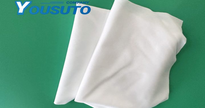
Semiconductor manufacturing—from wafer fabrication to chip assembly—relies on ultra-clean environments (ISO Class 1–5) where even 0.1μm particles or solvent residues can ruin 3nm–7nm microchips. Pre-wet cleanroom wipes, pre-impregnated with high-purity solvents (99.9% IPA, deionized water) or specialized cleaners, eliminate manual solvent mixing risks (particle contamination, inconsistent concentration) and ensure repeatable cleaning. Below are standardized application methods tailored to key semiconductor cleaning workflows.
1. Wafer Edge & Backside Cleaning (Pre-Lithography/Deposition)
Wafer edges and backsides accumulate particle debris, organic residues (from handling tools), and metal oxides—contaminants that migrate to the frontside during processing, causing pattern defects.
- Wipe Selection: Use 4”x4” pre-wet wipes with 99.9% electronic-grade IPA (low metal impurities ≤10 ppb) and static-dissipative fibers (surface resistance: 10⁶–10¹⁰ Ω). Avoid larger wipes to prevent solvent contact with the wafer frontside.
- Application Steps:
- Secure the wafer on a vacuum chuck (frontside down, edge exposed) in a laminar flow hood to block airborne particles.
- Fold the pre-wet wipe into a 1cm-wide strip to target only edges/backsides—minimizes over-wiping.
- Wipe the edge in a slow, continuous circular motion (1 full rotation) with light pressure (<0.5 psi)—prevents scratching thin dielectric layers.
- For the backside, use radial strokes (center to edge) with a fresh wipe section to avoid re-depositing particles.
- Key Requirement: Use 1 wipe per wafer—reuse transfers cross-contamination.
2. Photolithography Tool Optic Cleaning (Lenses, Reticles)
EUV scanners and photolithography tools depend on ultra-clean optics; a single 0.1μm particle on a lens distorts circuit patterns, ruining entire wafer batches.
- Wipe Selection: Choose pre-wet wipes with deionized water (for particle removal) or lens-grade IPA (for organic residues)—both meet SEMI C12 low-outgassing standards. Opt for ultra-fine microfiber (0.1μm diameter) to avoid scratching AR coatings.
- Application Steps:
- Power down the tool and purge the optic chamber with nitrogen to reduce airborne particles.
- Wear Class 10 cleanroom gloves; remove the reticle/lens per manufacturer guidelines (avoid touching optical surfaces).
- Fold the pre-wet wipe into a 2-layer pad (smooth side out) to minimize friction.
- Wipe the optic in a single linear stroke (not circular—prevents particle spreading) from edge to edge. Discard the wipe after 1 stroke—never reuse on optics.
- Follow with a dry high-density wipe to blot excess solvent—critical for EUV lenses (moisture damages performance).
3. Wafer Chuck & Tool Fixture Cleaning (Etching/Deposition Tools)
Wafer chucks (hold wafers during processing) and quartz fixtures accumulate process residues (photoresist, etch byproducts) and oil (from vacuum seals)—contaminants that cause wafer misalignment or defects.
- Wipe Selection: For ceramic chucks, use pre-wet wipes with 99% IPA (dissolves oil/residues); for quartz fixtures, use deionized water-based pre-wet wipes (prevents quartz degradation).
- Application Steps:
- Cool the tool to <30°C—hot surfaces evaporate solvent, leaving residues and increasing fire risk.
- Wipe chuck surfaces with a folded pre-wet wipe in spiral strokes (center to edge) to cover vacuum holes—use a wipe strip to clean hole interiors (prevents clogging).
- For quartz fixtures (e.g., wafer carriers), wipe slots with a thin wipe strip guided by tweezers—avoids damaging precision alignment features.
- Verify cleanliness with a portable particle counter (target: ≤1 particle ≥0.1μm per ft³) to meet ISO Class 1 standards.
4. Post-Bonding Chip Cleaning (Packaging Stage)
After die bonding, chips accumulate flux residues and adhesive smudges—contaminants that impair electrical connectivity or cause thermal issues.
- Wipe Selection: Use pre-wet wipes with a mild, semiconductor-grade flux remover (compatible with copper/AlSiC substrates) and lint-free polyester fibers.
- Application Steps:
- Place the bonded chip on an ESD-safe mat; ground yourself with a wrist strap.
- Fold the pre-wet wipe into a small pad and dab (not wipe) flux residues—wiping risks dislodging the die.
- For adhesive smudges, hold the wipe against the spot for 5 seconds (lets remover dissolve the adhesive) before gentle dabbing.
- Follow with a dry anti-static wipe to remove remover residues—ensures no film impacts chip performance.
Critical Compliance & Safety Notes
- Solvent Purity: All pre-wet wipes must meet SEMI C30 standards—impurities (metals, organics) cause wafer defects.
- Storage: Keep wipes in sealed, nitrogen-flushed containers to prevent solvent evaporation (dried wipes lose efficacy).
- Waste Disposal: Discard used wipes in fire-resistant bins—IPA/flux removers are flammable; segregate to avoid cross-contamination.
By following these methods, pre-wet cleanroom wipes maintain semiconductor cleanliness, reduce defect rates by 30–40%, and protect high-value equipment—critical for producing reliable, next-generation microchips.
