PCB soldering areas—including solder joints, component leads, and pad surfaces—often accumulate flux residues, rosin, and thermal oxidation byproducts post-soldering. These contaminants cause poor electrical conductivity, corrosion, or adhesion issues for subsequent assembly steps. IPA (Isopropyl Alcohol) wipes are the industry standard for cleaning these areas, as IPA effectively dissolves flux/rosin while being compatible with most PCB substrates and components. Below is a detailed guide to their application, covering best practices, safety, and results.
1. Key Benefits of IPA Wipes for PCB Soldering Area Cleaning
Before diving into application steps, it’s critical to understand why IPA wipes outperform other cleaning methods (e.g., bulk solvent + rags) for soldering areas:
- Targeted Flux Dissolution: IPA (especially 99% purity) breaks down both no-clean and rosin-based flux residues—common byproducts of wave soldering or reflow soldering. It penetrates small gaps between component leads and pads, removing hidden residues that rags or brushes miss.
- Lint-Free Precision: High-quality IPA wipes use continuous-filament polyester or microfiber, shedding ≤1 fiber per use. This avoids fiber contamination of solder joints—critical for fine-pitch components (0.4mm pitch or smaller), where stray fibers can cause short circuits.
- Fast Evaporation: IPA evaporates quickly (within 10–15 seconds at room temperature), leaving no solvent streaks or moisture that could damage PCB laminates (e.g., FR-4) or corrode metal pads.
- ESD Safety (Anti-Static Variants): Anti-static IPA wipes (surface resistance: 10⁶–10¹¹ Ω) dissipate static charge during cleaning, protecting ESD-sensitive components (e.g., IC chips, sensors) near soldering areas from discharge damage.
2. Step-by-Step Application Process
Follow this standardized workflow to clean PCB soldering areas effectively without damaging components:
Step 1: Pre-Clean Preparation
- Cool the PCB: Wait for the soldered PCB to cool to <40°C (room temperature). Cleaning hot PCBs (≥60°C) causes IPA to evaporate too quickly, leaving incomplete residue removal; it also risks thermal shock to components.
- Select the Right IPA Wipe:
- For rosin-based flux (thicker residues): Use 99% electronic-grade IPA wipes—higher purity dissolves heavy residues faster.
- For no-clean flux (lighter residues): 70% IPA wipes work well (the water content helps lift residue without damaging delicate components like LEDs or capacitors).
- For ESD-sensitive areas (e.g., near microchips): Choose anti-static IPA wipes to prevent charge buildup.
- Set Up a Safe Workspace:
- Work in a well-ventilated area (fume hood or open window) to disperse IPA vapors (flammable and irritating to airways).
- Remove ignition sources (e.g., heat guns, soldering irons) and place the PCB on an ESD-safe mat to ground static.
Step 2: Wipe Application Technique
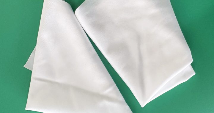
- Fold the Wipe for Precision: Fold the IPA wipe into a 4-layer pad. This creates a dense cleaning surface (reduces fiber shedding) and allows you to use a fresh layer for each section of the PCB—preventing re-depositing residues.
- Clean Soldering Areas with Controlled Strokes:
- Solder Joints/Component Leads: Wipe in a slow, linear motion along the length of the component (e.g., from one end of a resistor to the other). Apply light pressure (<1 psi)—excessive force can bend delicate leads or dislodge newly soldered components.
- Pad Surfaces (Bare or Component-Free): Wipe in overlapping horizontal strokes to cover the entire pad area. Focus on oxidized pads (dull, discolored surfaces)—IPA helps remove light oxidation, restoring pad conductivity.
- Tight Gaps (e.g., QFP/BGA Components): Tear a small strip from the wipe and use tweezers to guide it between component pins. This removes residue trapped in gaps that a full wipe pad can’t reach.
Step 3: Post-Clean Inspection & Protection
- Verify Residue Removal: Inspect the soldering areas under a 10–20x magnifying glass or digital microscope. Look for:
- Glossy flux residues (indicates incomplete cleaning)—reclean with a fresh IPA wipe section.
- Fiber debris (from low-quality wipes)—remove with a gentle blast of static-neutralized compressed air.
- Component damage (e.g., bent leads, lifted pads)—address before proceeding with further assembly.
- Dry the PCB (If Needed): For 70% IPA wipes (higher water content), use a dry, lint-free anti-static wipe to blot any remaining moisture on solder joints. This prevents water spots or potential corrosion.
- Store the Cleaned PCB: Place the PCB in an anti-static bag or container immediately after cleaning. Avoid touching soldering areas with bare hands—skin oils reintroduce contaminants and can cause pad oxidation over time.
3. Critical Do’s and Don’ts
- Do: Use only electronic-grade IPA wipes (meets SEMI C30 standards for low impurities). Household IPA may contain additives (e.g., fragrances, moisturizers) that leave residues on PCBs.
- Don’t: Clean PCBs with cracked or damaged laminates—IPA can seep into cracks and delaminate the PCB structure.
- Do: Dispose of used IPA wipes in a fire-resistant bin. Used wipes retain flammable IPA and pose a fire risk if left near heat sources.
- Don’t: Reuse IPA wipes for soldering area cleaning. Used wipes trap flux residues and will spread contaminants to other parts of the PCB.
By using IPA wipes correctly, PCB soldering areas remain clean, conductive, and free of corrosion—ensuring reliable electrical performance, reducing post-assembly failures, and complying with electronics manufacturing standards (e.g., IPC-A-610).