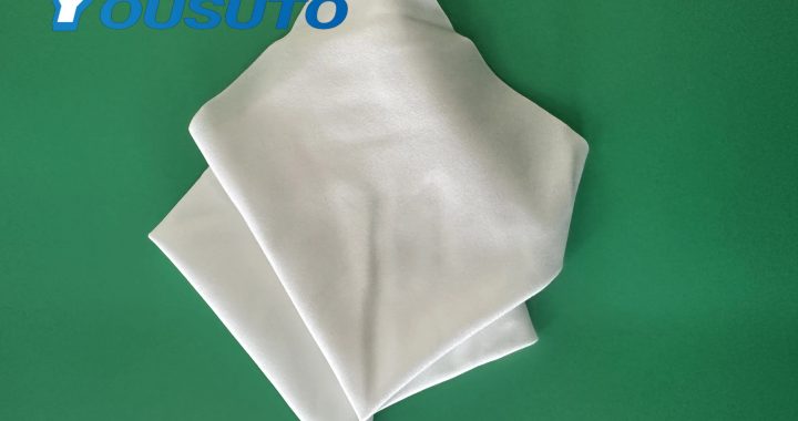
In high-volume electronics manufacturing—where consistent cleaning of PCBs (printed circuit boards), semiconductors, and connectors directly impacts product yield—standardized IPA wipe cleaning processes eliminate variability, reduce defects, and ensure compliance with industry standards (e.g., IPC-A-610). Below is a real-world case study of how a global electronics contract manufacturer (CM) implemented a standardized IPA wipe workflow to address inconsistent flux removal, ESD risks, and cross-contamination—resulting in a 35% reduction in cleaning-related defects.
Background: The Challenge of Unstandardized Cleaning
Before implementation, the CM relied on ad-hoc IPA wipe use by technicians, leading to three critical issues:
- Inconsistent Flux Removal: Technicians used varying IPA concentrations (70% vs. 99%) and wipe pressures, leaving 15–20% of PCBs with residual flux (a leading cause of electrical leakage in finished devices).
- ESD Damage: Ungrounded technicians and non-ESD-safe wipes generated static charges (200–500V), causing 8% of semiconductor chips to fail post-cleaning.
- Cross-Contamination: Reused IPA wipes transferred solder debris between PCBs, resulting in 10% of boards requiring rework.
Step 1: Define Standardized Process Parameters
The CM collaborated with IPA wipe manufacturers and IPC experts to establish strict process parameters, tailored to their two core cleaning tasks: post-soldering flux removal and connector pin cleaning.
| Process Step | Post-Soldering Flux Removal (PCBs) | Connector Pin Cleaning (Semiconductor Modules) |
|---|---|---|
| IPA Wipe Specification | Pre-moistened, 99% high-purity IPA, ESD-safe (10⁶–10¹¹ Ω), ISO Class 5 lint-free (polyester microfiber) | Pre-moistened, 70% IPA (for oil dissolution), ESD-safe, 4”x4” size (for precision access) |
| Operator Prep | Wear ESD wrist strap + nitrile gloves; ground workbench to <100V static charge | Same as above; add anti-static shoe covers for module assembly areas |
| Wiping Technique | Fold wipe into 4-layer pad; wipe PCB in single horizontal strokes (50% overlap); 1–2 psi pressure | Fold wipe into strip; gently drag along pin rows (1 stroke per row); avoid bending pins |
| Post-Clean Check | Inspect under 10x magnification for flux residues; test static charge with ESD meter (<100V) | Inspect pins for oil/debris with 20x magnification; use continuity tester to confirm no pin damage |
| Waste Disposal | Discard used wipes in fire-resistant, ESD-safe bins; empty after each shift | Same as above; separate connector wipes from PCB wipes to avoid cross-contamination |
Step 2: Technician Training & Documentation
To ensure adherence, the CM implemented:
- Hands-On Training: 2-hour sessions where technicians practiced the standardized workflow on dummy PCBs/modules, with real-time feedback from IPC-certified trainers.
- Visual Work Instructions (VWIs): Posters at each cleaning station showing wipe folding techniques, pressure guides, and inspection checklists (with photos of “good vs. bad” cleaning results).
- Digital Logging: Technicians logged each cleaning task (PCB lot number, wipe lot number, post-clean check results) in a cloud-based system for traceability.
Step 3: Process Validation & Continuous Improvement
After 4 weeks of implementation, the CM validated the process with key metrics:
- Flux Residue Rate: Dropped from 18% to 3% (meeting IPC-A-610 Class 3 requirements for high-reliability electronics).
- ESD-Related Failures: Reduced from 8% to 0.5% (thanks to ESD-safe wipes and grounded operators).
- Rework Rate: Fell from 10% to 2% (eliminated cross-contamination via single-use wipes and separate waste bins).
To sustain improvements, the CM conducts monthly audits:
- Randomly test 5% of cleaned PCBs/modules for residues and static.
- Survey technicians for workflow pain points (e.g., wipe size, packaging) and adjust parameters (e.g., switching to 6”x6” wipes for larger PCBs based on feedback).
Key Takeaways from the Case Study
This standardized IPA wipe process demonstrates that:
- Parameter Consistency (IPA concentration, wipe type, technique) eliminates human error as a source of defects.
- ESD Integration (safe wipes + operator grounding) protects sensitive components from static damage.
- Traceability (digital logging) enables rapid root-cause analysis if issues arise.
For electronics manufacturers, medical device makers, or any facility relying on precision cleaning, this case study provides a scalable blueprint for implementing a standardized IPA wipe process—turning a variable task into a repeatable, high-quality step in production.
