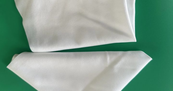
Cleaning wipes are critical in semiconductor cleanrooms to maintain particle-free surfaces, protect sensitive devices, and comply with strict ISO standards.
Key Features:
-
Lint-Free and Non-Abrasive: Prevents fiber contamination and scratches on delicate wafers and PCBs.
-
Antistatic Properties: Reduces electrostatic discharge (ESD) risks for sensitive semiconductor components.
-
High Absorbency: Efficiently removes oils, dust, and residues with fewer wipes.
-
Chemical Compatibility: Safe for use with IPA, deionized water, and approved cleaning agents.
Application Case:
-
Wafer Cleaning: Wipes remove microscopic particles and residues without damaging surfaces.
-
PCB Maintenance: Efficiently cleans flux residues and dust during assembly and inspection.
-
Semiconductor Equipment: Maintains particle-free workstations and handling tools.
-
Optical Inspection: Keeps sensors and lenses clean for accurate measurements.
Benefits:
-
Maintains Cleanroom Standards: Supports ISO Class 100–1000 compliance.
-
Protects Sensitive Devices: Antistatic, lint-free wipes reduce ESD and contamination.
-
Improves Efficiency: High absorbency and pre-wetted options streamline cleaning tasks.
-
Reduces Cross-Contamination: Single-use wipes ensure safe, residue-free cleaning.