High-density cleanroom wipes are critical in semiconductor manufacturing, where particle control and surface cleanliness directly affect yield and device performance.
Key Features:
-
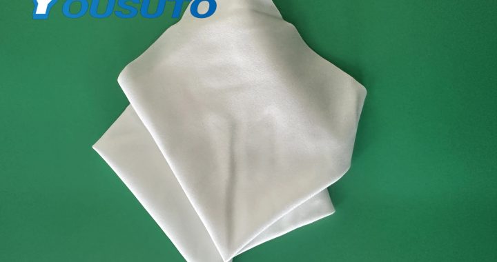
Tightly Woven Fibers: Capture microscopic particles to maintain ultra-clean surfaces.
-
High Absorbency: Efficiently removes residues, oils, and spills from sensitive wafers and equipment.
-
Lint-Free and Non-Abrasive: Protects delicate wafers, photomasks, and semiconductor components.
-
Chemical Compatibility: Resistant to IPA, deionized water, and other approved cleaning agents.
Applications:
-
Wafer Cleaning: Removes particles and residues without scratching surfaces.
-
Photomask Maintenance: Ensures precise patterning by eliminating contaminants.
-
Equipment Wiping: Cleans tools, benches, and robotic arms in production lines.
-
Cleanroom Surfaces: Maintains ISO Class 1–5 standards in semiconductor fabs.
Benefits:
-
Enhanced Yield and Quality: Reduces defects caused by particle contamination.
-
Protects Sensitive Components: Non-abrasive and lint-free construction prevents damage.
-
Improves Cleaning Efficiency: High absorbency decreases wipe consumption and labor.